SLOSE89A November   2021  – March 2022 THS4541-DIE

PRODUCTION DATA  

  1. Features
  2. Applications
  3. Description
  4. Revision History
  5. Bare Die Information
  6. Pin Configuration and Functions
  7. Specifications
    1. 7.1 Absolute Maximum Ratings
    2. 7.2 Recommended Operating Conditions
    3. 7.3 Electrical Characteristics: (Vs+) - Vs- = 5 V
    4. 7.4 Typical Characteristics 5-V Single Supply
    5. 7.5 Typical Characteristics: 3-V to 5-V Supply Range
  8. Detailed Description
    1. 8.1 Overview
      1. 8.1.1 Terminology and Application Assumptions
    2. 8.2 Functional Block Diagram
    3. 8.3 Feature Description
      1. 8.3.1 Differential I/O
      2. 8.3.2 Power-Down Control Pin (PD)
        1. 8.3.2.1 Operating the Power Shutdown Feature
      3. 8.3.3 Input Overdrive Operation
    4. 8.4 Device Functional Modes
      1. 8.4.1 Operation from Single-Ended Sources to Differential Outputs
  9. Application and Implementation
    1. 9.1 Application Information
    2. 9.2 Typical Applications
      1. 9.2.1 Interfacing to High-Performance ADCs
        1. 9.2.1.1 Design Requirements
        2. 9.2.1.2 Detailed Design Procedure
        3. 9.2.1.3 Application Curve
  10. 10Power Supply Recommendations
  11. 11Layout
    1. 11.1 Layout Guidelines
  12. 12Device and Documentation Support
    1. 12.1 Device Support
      1. 12.1.1 Development Support
        1. 12.1.1.1 TINA Simulation Model Features
    2. 12.2 Documentation Support
      1. 12.2.1 Related Documentation
    3. 12.3 Receiving Notification of Documentation Updates
    4. 12.4 Support Resources
    5. 12.5 Trademarks
    6. 12.6 Electrostatic Discharge Caution
    7. 12.7 Glossary
  13. 13Mechanical, Packaging, and Orderable Information

Package Options

Mechanical Data (Package|Pins)
  • Y|0
Thermal pad, mechanical data (Package|Pins)
Orderable Information

Typical Characteristics: 3-V to 5-V Supply Range

at Vs+ = 3 V and 5 V, Vs– = GND, Vocm is open, 50-Ω single-ended input to differential output, RF = 402 Ω,Gain = 2 V/V, Rload = 500 Ω, and TA ≈ 25°C (unless otherwise noted)
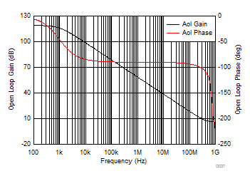
GUID-91445852-7E4A-4559-8B8D-523DD39455C9-low.gif
Figure 7-11 Main Amplifier Differential Open-Loop Gain and Phase vs Frequency
GUID-883140B3-79FB-46B3-BAD0-F33E2770259E-low.gif
Figure 7-13 Input Spot Noise Over Frequency
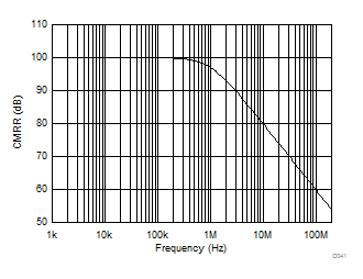
GUID-930518F0-E340-4AF5-A6F7-18D8D38620AB-low.gif
Common-mode in to differential out, gain of 2 simulation
Figure 7-15 CMRR Over Frequency
GUID-F299392B-CF64-4AE2-ABD1-D51F3FBA0A8A-low.gif
Figure 7-17 Common-Mode, Small- and Large-Signal Response (Vocm pin driven)
GUID-20210623-CA0I-M9DC-QV5Q-6NCPM4KQK83G-low.png
Total of 4618 units, At Vs = 5V: μ = -35.1μV, σ = 38.9μV
Figure 7-19 Input Offset Voltage
GUID-FAC69C7D-5BF7-4791-9BC9-2B909AB62660-low.gif
Maximum differential output swing, Vocm at midsupply
Figure 7-21 Maximum Vopp vs Rload
Vocm input floating, Total of 4618 units,
At Vs = 5V: μ = 6.8mV, σ = 3.9mV
Figure 7-23 Common-Mode Output Offset from Vs+ / 2 Default Value
GUID-72B191FD-9056-4755-A22E-CCE72AE063AC-low.gif
10 MHz, 1-Vpp input single to differential gain of 2
Figure 7-25 PD Turn On Waveform
GUID-92BA6D0B-7C74-4539-8E61-BBC0D57B0F99-low.gif
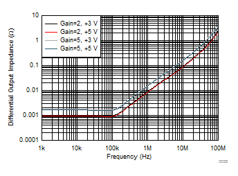
Single-ended input to differential output, simulated differential output impedance, (closed-loop) gain of 2 and 5
Figure 7-12 Closed-Loop Output Impedance
GUID-E81C79B5-08A4-4F41-93C4-0523CEDFCE7F-low.gif
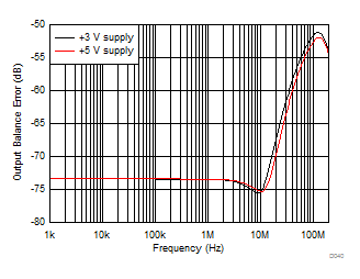
Single-ended input to differential output, gain of 2, simulated with 1% resistor, worst-case mismatch
Figure 7-14 Output Balance Error Over Frequency
GUID-9B5158FB-3353-47B5-97D2-5981EED8340E-low.gif
Single-ended to differential, gain of 2
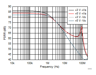
PSRR simulated to differential output
Figure 7-16 PSRR Over Frequency
GUID-2CB62603-82C0-4298-A78B-F432B9440F50-low.gif
Vocm input either driven to mid-supply by low impedance source, or allowed to float and default to mid-supply
Figure 7-18 Output Common-Mode Noise
Total of 4618 units, At Vs = 5V: μ = 16.7nA, σ = 62.3nA
Figure 7-20 Input Offset Current
GUID-8D765DFC-360B-451F-8D09-D8A8497C783A-low.gif
Figure 7-22 Supply Current vs PD Voltage
Total of 4618 units, At Vs = 5V: μ = -0.3mV, σ = 1.3mV
Figure 7-24 Common-Mode Output Offset from Driven Vocm
GUID-ABB2CF0B-208D-430A-9059-A1D6BD62006A-low.gif
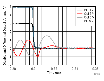
10 MHz, 1-VPP input single to differential gain of 2
Figure 7-26 PD Turn Off Waveform