SLOS375B August 2014 – February 2024 THS4541
PRODUCTION DATA
- 1
- 1 Features
- 2 Applications
- 3 Description
- 4 Device Comparison Table
- 5 Pin Configuration and Functions
-
6 Specifications
- 6.1 Absolute Maximum Ratings
- 6.2 ESD Ratings
- 6.3 Recommended Operating Conditions
- 6.4 Thermal Information
- 6.5 Electrical Characteristics: (Vs+) – Vs– = 5 V
- 6.6 Electrical Characteristics: (Vs+) – Vs– = 3 V
- 6.7 Typical Characteristics 5-V Single Supply
- 6.8 Typical Characteristics: 3-V Single Supply
- 6.9 Typical Characteristics: 3-V to 5-V Supply Range
-
7 Parameter Measurement Information
- 7.1 Example Characterization Circuits
- 7.2 Frequency-Response Shape Factors
- 7.3 I/O Headroom Considerations
- 7.4 Output DC Error and Drift Calculations and the Effect of Resistor Imbalances
- 7.5 Noise Analysis
- 7.6 Factors Influencing Harmonic Distortion
- 7.7 Driving Capacitive Loads
- 7.8 Thermal Analysis
-
8 Detailed Description
- 8.1 Overview
- 8.2 Functional Block Diagram
- 8.3 Feature Description
- 8.4
Device Functional Modes
- 8.4.1
Operation from Single-Ended Sources to Differential Outputs
- 8.4.1.1 AC-Coupled Signal Path Considerations for Single-Ended Input to Differential Output Conversion
- 8.4.1.2 DC-Coupled Input Signal Path Considerations for Single-Ended to Differential Conversion
- 8.4.1.3 Resistor Design Equations for the Single-Ended to Differential Configuration of the FDA
- 8.4.1.4 Input Impedance for the Single-Ended to Differential FDA Configuration
- 8.4.2 Differential-Input to Differential-Output Operation
- 8.4.1
Operation from Single-Ended Sources to Differential Outputs
- 9 Application and Implementation
- 10Device and Documentation Support
- 11Revision History
- 12Mechanical, Packaging, and Orderable Information
Package Options
Refer to the PDF data sheet for device specific package drawings
Mechanical Data (Package|Pins)
- RUN|10
- RGT|16
Thermal pad, mechanical data (Package|Pins)
Orderable Information
9.2.1 Designing Attenuators
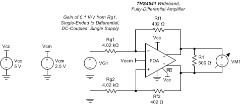
 Figure 9-1 Divide-by-10 Attenuator Application for the THS4541