at Vs+ = 5 V, Vs– = GND, Vocm is open,
50-Ω single-ended input to differential output, gain = 2 V/V, Rload = 500 Ω, and TA
≈ 25°C (unless otherwise noted)
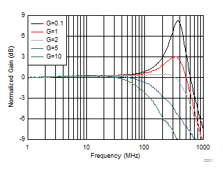
 Figure 6-1 Small-Signal Frequency Response vs Gain
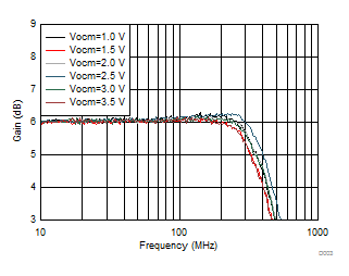
| Vout = 100 mVPP
, see Figure 7-1 with Vocm adjusted |
Figure 6-3 Small-Signal Frequency Response vs Vocm
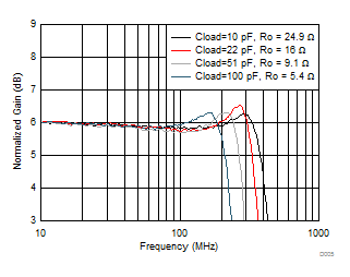
| 100 mVPP at load, Av = 2 (see Figure 7-11), two series Ro added at output before Cload |
Figure 6-5 Small-Signal Frequency Response vs Cload
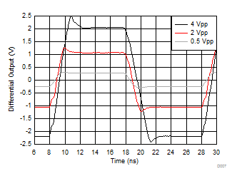
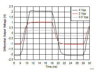
| 50-MHz input, 0.3-ns input edge rate, single-ended to
differential output, DC coupled,see Figure 7-3 |
Figure 6-7 Small- and Large-Signal Step Response
| G = 5 V/V, 50-MHz input, 0.3-ns input edge rate,
single-ended input to differential output, see Figure 7-3 |
Figure 6-9 Small- and Large-Signal Step Response
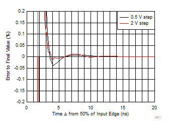
| Simulated with 2-ns input
transition time (see Figure 7-3) |
| |
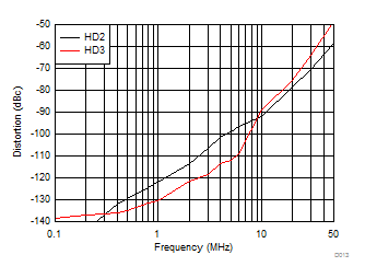
Figure 6-11 Small- and Large-Signal Step Settling Time Figure 6-13 Harmonic Distortion Over Frequency
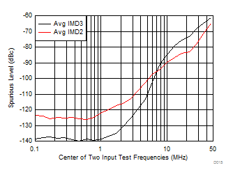
 Figure 6-15 IMD2
and IM3 Over Frequency
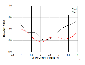
 Figure 6-17 Harmonic Distortion vs Vocm
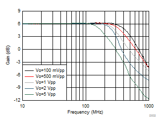
 Figure 6-2 Frequency Response vs Vopp
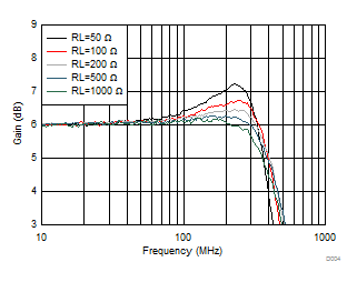
 Figure 6-4 Small-Signal Frequency Response vs Rload (RL)
| Ro is two series output resistors to a differential
Cload in parallel with 500 Ω, see Figure 7-11 and Table 8-1 |
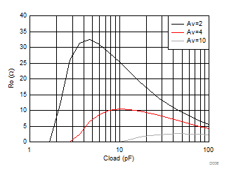
Figure 6-6 Recommended Ro vs Cload
Av = 2 , 500-mVPP output into 22-pF
Cload,
see Figure 7-11 |
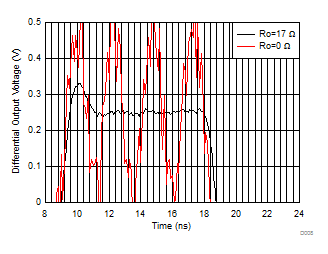
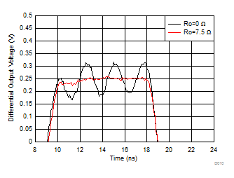
Figure 6-8 Step
Response into Capacitive Load Figure 6-10 Step
Response into Capacitive Load
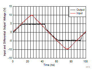
Single-ended to differential gain of 2 (see Figure 7-3),
2 × input
overdrive |
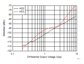
Figure 6-12 Overdrive Recovery Performance Figure 6-14 Harmonic Distortion vs Output Swing
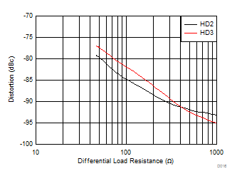
 Figure 6-16 Harmonic Distortion vs Rload
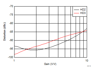
 Figure 6-18 Harmonic Distortion vs Gain
