SBOS778D April   2016  – April 2021 THS4551

PRODUCTION DATA  

  1. Features
  2. Applications
  3. Description
  4. Revision History
  5. Companion Devices
  6. Pin Configuration and Functions
  7. Specifications
    1. 7.1 Absolute Maximum Ratings
    2. 7.2 ESD Ratings
    3. 7.3 Recommended Operating Conditions
    4. 7.4 Thermal Information
    5. 7.5 Electrical Characteristics: (VS+) – (VS–) = 5 V
    6. 7.6 Electrical Characteristics: (VS+) – (VS–) = 3 V
    7. 7.7 Typical Characteristics: (VS+) – (VS–) = 5 V
    8. 7.8 Typical Characteristics: (VS+) – (VS–) = 3 V
    9. 7.9 Typical Characteristics: 3-V to 5-V Supply Range
  8. Parameter Measurement Information
    1. 8.1 Example Characterization Circuits
    2. 8.2 Output Interface Circuit for DC-Coupled Differential Testing
    3. 8.3 Output Common-Mode Measurements
    4. 8.4 Differential Amplifier Noise Measurements
    5. 8.5 Balanced Split-Supply Versus Single-Supply Characterization
    6. 8.6 Simulated Characterization Curves
    7. 8.7 Terminology and Application Assumptions
  9. Detailed Description
    1. 9.1 Overview
    2. 9.2 Functional Block Diagram
    3. 9.3 Feature Description
      1. 9.3.1 Differential Open-Loop Gain and Output Impedance
      2. 9.3.2 Setting Resistor Values Versus Gain
      3. 9.3.3 I/O Headroom Considerations
      4. 9.3.4 Output DC Error and Drift Calculations and the Effect of Resistor Imbalances
    4. 9.4 Device Functional Modes
      1. 9.4.1 Operation from Single-Ended Sources to Differential Outputs
        1. 9.4.1.1 AC-Coupled Signal Path Considerations for Single-Ended Input to Differential Output Conversions
        2. 9.4.1.2 DC-Coupled Input Signal Path Considerations for Single-Ended to Differential Conversions
      2. 9.4.2 Operation from a Differential Input to a Differential Output
        1. 9.4.2.1 AC-Coupled, Differential-Input to Differential-Output Design Issues
        2. 9.4.2.2 DC-Coupled, Differential-Input to Differential-Output Design Issues
      3. 9.4.3 Input Overdrive Performance
  10. 10Application and Implementation
    1. 10.1 Application Information
      1. 10.1.1 Noise Analysis
      2. 10.1.2 Factors Influencing Harmonic Distortion
      3. 10.1.3 Driving Capacitive Loads
      4. 10.1.4 Interfacing to High-Performance Precision ADCs
      5. 10.1.5 Operating the Power Shutdown Feature
      6. 10.1.6 Designing Attenuators
      7. 10.1.7 The Effect of Adding a Feedback Capacitor
    2. 10.2 Typical Applications
      1. 10.2.1 An MFB Filter Driving an ADC Application
        1. 10.2.1.1 Design Requirements
        2. 10.2.1.2 Detailed Design Procedure
        3. 10.2.1.3 Application Curves
      2. 10.2.2 Differential Transimpedance Output to a High-Grade Audio PCM DAC Application
        1. 10.2.2.1 Design Requirements
        2. 10.2.2.2 Detailed Design Procedure
        3. 10.2.2.3 Application Curves
      3. 10.2.3 ADC3k Driver with a 2nd-Order RLC Interstage Filter Application
        1. 10.2.3.1 Design Requirements
        2. 10.2.3.2 Detailed Design Procedure
        3. 10.2.3.3 Application Curve
  11. 11Power Supply Recommendations
    1. 11.1 Thermal Analysis
  12. 12Layout
    1. 12.1 Layout Guidelines
      1. 12.1.1 Board Layout Recommendations
    2. 12.2 Layout Example
    3. 12.3 EVM Board
  13. 13Device and Documentation Support
    1. 13.1 Device Support
      1. 13.1.1 TINA-TI Simulation Model Features
    2. 13.2 Documentation Support
      1. 13.2.1 Related Documentation
    3. 13.3 Receiving Notification of Documentation Updates
    4. 13.4 Support Resources
    5. 13.5 Trademarks
    6. 13.6 Electrostatic Discharge Caution
    7. 13.7 Glossary
  14. 14Mechanical, Packaging, and Orderable Information

Package Options

Mechanical Data (Package|Pins)
Thermal pad, mechanical data (Package|Pins)
Orderable Information

EVM Board

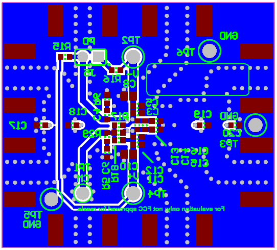
Figure 12-2 and Figure 12-3 show the layout of the top and bottom layers of the THS4551DGKEVM evaluation module, respectively.
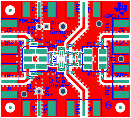
GUID-91D1FD87-6210-42F0-80A4-501ED5777F63-low.png Figure 12-2 THS4551DGKEVM Top Layer
GUID-4291D54A-1A7F-42B7-B4ED-F7DB2BF5FB70-low.png Figure 12-3 THS4551DGKEVM Bottom Layer