SBOS831B December 2016 – June 2021 THS4552
PRODUCTION DATA
- 1 Features
- 2 Applications
- 3 Description
- 4 Revision History
- 5 Pin Configuration and Functions
-
6 Specifications
- 6.1 Absolute Maximum Ratings
- 6.2 ESD Ratings
- 6.3 Recommended Operating Conditions
- 6.4 Thermal Information
- 6.5 Electrical Characteristics: (VS+) – (VS–) = 5 V
- 6.6 Electrical Characteristics: (VS+) – (VS–) = 3 V
- 6.7 Typical Characteristics: (VS+) – (VS–) = 5 V
- 6.8 Typical Characteristics: (VS+) – (VS–) = 3 V
- 6.9 Typical Characteristics: 3 V to 5 V Supply Range
-
7 Parameter Measurement Information
- 7.1 Example Characterization Circuits
- 7.2 Output Interface Circuit for DC-Coupled Differential Testing
- 7.3 Output Common-Mode Measurements
- 7.4 Differential Amplifier Noise Measurements
- 7.5 Balanced Split-Supply Versus Single-Supply Characterization
- 7.6 Simulated Characterization Curves
- 7.7 Terminology and Application Assumptions
- 8 Detailed Description
-
9 Application and Implementation
- 9.1
Application Information
- 9.1.1 Noise Analysis
- 9.1.2 Factors Influencing Harmonic Distortion
- 9.1.3 Driving Capacitive Loads
- 9.1.4 Interfacing to High-Performance Precision ADCs
- 9.1.5 Operating the Power Shutdown Feature
- 9.1.6 Channel-to-Channel Crosstalk
- 9.1.7 Channel-to-Channel Mismatch
- 9.1.8 Designing Attenuators
- 9.1.9 The Effect of Adding a Feedback Capacitor
- 9.2 Typical Applications
- 9.1
Application Information
- 10Power Supply Recommendations
- 11Layout
- 12Device and Documentation Support
- 13Mechanical, Packaging, and Orderable Information
Package Options
Mechanical Data (Package|Pins)
Thermal pad, mechanical data (Package|Pins)
- RTW|24
Orderable Information
9.2.3.3 Application Curve
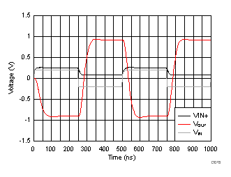
Driving a 2 MHz ±0.2 V square wave into this circuit (using a TINA-TI™ simulation file for the circuit of Figure 9-20) gives the response shown in Figure 9-21 at the ADC. The red trace is a –1 dBFS, 1.8 VPP square wave at the ADC input pins. The gray trace is the input signal at the RT termination resistor. The black trace is the common-mode voltage at the FDA input pins. Note that the input pin voltage swing stays above ground and in range for this bipolar input, single, 3.3 V supply design.
 Figure 9-21 Time-Domain Waveform
Unbuffered pipeline ADCs draw a clock-rate-dependent input common-mode current. For the ADC3241, this input current is specified as 1.5 µA per MSPS. Operating at 25 MSPS, the common-mode current drops the common-mode voltage from 0.95 V at the THS4552 outputs by 37.5 µA × 45.8 Ω = 1.7 mV to 0.9483 V. This value is well within the allowed ±25 mV common-mode deviation from the ADC VCM output. Consider this effect carefully when using higher resistor values in the interface at the ADC.