SBOS874D August 2017 – February 2021 THS4561
PRODUCTION DATA
- 1 Features
- 2 Applications
- 3 Description
- 4 Revision History
- 5 Device Comparison Table
- 6 Pin Configuration and Functions
-
7 Specifications
- 7.1 Absolute Maximum Ratings
- 7.2 ESD Ratings
- 7.3 Recommended Operating Conditions
- 7.4 Thermal Information
- 7.5 Electrical Characteristics: VS+ – VS– = 5 V to 12 V
- 7.6 Typical Characteristics: (VS+) – (VS–) = 12 V
- 7.7 Typical Characteristics: (VS+) – (VS–) = 5 V
- 7.8 Typical Characteristics: (VS+) – (VS–) = 3 V
- 7.9 Typical Characteristics: (VS+) – (VS–) = 3-V to 12-V Supply Range
-
8 Parameter Measurement Information
- 8.1 Example Characterization Circuits
- 8.2 Output Interface Circuit for DC-Coupled Differential Testing
- 8.3 Output Common-Mode Measurements
- 8.4 Differential Amplifier Noise Measurements
- 8.5 Balanced Split-Supply Versus Single-Supply Characterization
- 8.6 Simulated Characterization Curves
- 8.7 Terminology and Application Assumptions
- 9 Detailed Description
- 10Application and Implementation
- 11Power Supply Recommendations
- 12Layout
- 13Device and Documentation Support
- 14Mechanical, Packaging, and Orderable Information
Package Options
Mechanical Data (Package|Pins)
Thermal pad, mechanical data (Package|Pins)
Orderable Information
10.1.5 Input Overdrive Performance
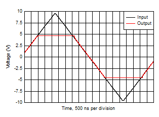
Figure 10-5 and Figure 10-6 show a 2-V and a 2X output overdrive triangular waveform, respectively, for the THS4561. When the output maximum swing is reached at approximately the supply values, increasing input voltage beyond this condition turns on the internal protection diodes across the two input pins. The internal protection diodes are two diodes in series in both polarities. This feature clamps the maximum differential voltage across the inputs to approximately 1.5 V when the output is limited at the supplies but the input exceeds the available range. The input resistors on both sides limit the current flow in the internal diodes under these conditions.

| VS = 12 V, Single-ended to differential gain of 2, 2-V output overdrive, overdrive recovery = 250 ns |

| VS = 5 V, Single-ended to differential gain of 2, 2x input overdrive, overdrive recovery = 210 ns |