SBOS758F April 2016 – June 2024 THS6212
PRODUCTION DATA
- 1
- 1 Features
- 2 Applications
- 3 Description
- 4 Pin Configuration and Functions
- 5 Specifications
- 6 Detailed Description
- 7 Application and Implementation
- 8 Device and Documentation Support
- 9 Revision History
- 10Mechanical, Packaging, and Orderable Information
Package Options
Refer to the PDF data sheet for device specific package drawings
Mechanical Data (Package|Pins)
- RHF|24
Thermal pad, mechanical data (Package|Pins)
Orderable Information
7.2.1.3 Application Curves
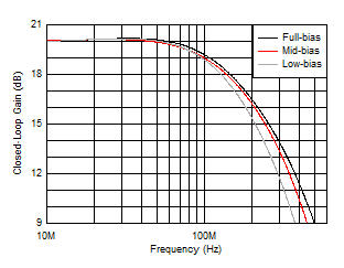
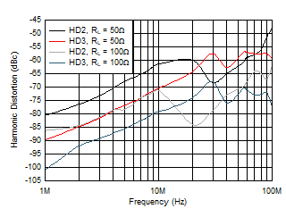
Figure 7-2 and Figure 7-3 show the frequency response and distortion performance of the circuit in Figure 7-1. The measurements are made with a load resistor (RL) of 100 Ω, and at room temperature. Figure 7-2 is measured using the three different device power modes, and the distortion measurements in Figure 7-3 are made at an output voltage level of 2 VPP.
 Figure 7-2 Frequency Response
 Figure 7-3 Harmonic Distortion