SBOS974F August 2019 – December 2024 THS6222
PRODUCTION DATA
- 1
- 1 Features
- 2 Applications
- 3 Description
- 4 Pin Configuration and Functions
- 5 Specifications
- 6 Detailed Description
- 7 Application and Implementation
- 8 Device and Documentation Support
- 9 Revision History
- 10Mechanical, Packaging, and Orderable Information
Package Options
Refer to the PDF data sheet for device specific package drawings
Mechanical Data (Package|Pins)
- RGT|16
- YS|0
- RHF|24
Thermal pad, mechanical data (Package|Pins)
- RGT|16
Orderable Information
6.3.4 Breakdown Supply Voltage
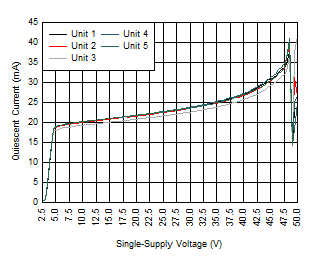
To estimate the margin beyond the maximum supply voltage specified in the Absolute Maximum Ratings table and exercise the robustness of the device, several typical units were tested beyond the specifications in the Absolute Maximum Ratings table. Figure 6-5 shows the configuration used for the test. The supply voltage, VS, was swept manually and quiescent current was recorded at each 0.5-V supply voltage increment. Figure 6-6 shows the results of the single-supply voltage where the typical units started breaking. Under a similar configuration as the one shown in Figure 6-5, a unit was subjected to VS = 42 V for 168 hours and tested for quiescent current at the beginning and at the end of the test. There was no notable difference in the quiescent current before and after the 168 hours of testing and the device did not show any signs of damage or abnormality.
The primary objective of these tests was to estimate the margins of robustness for typical devices and does not imply performance or maximum limits beyond those specified in the Absolute Maximum Ratings and Recommended Operating Conditions tables.
 Figure 6-5 Breakdown Supply Voltage Test Configuration
 Figure 6-6 Typical Device Breakdown Supply Voltage (TA = 27°C)