SBOS974F August 2019 – December 2024 THS6222
PRODUCTION DATA
- 1
- 1 Features
- 2 Applications
- 3 Description
- 4 Pin Configuration and Functions
- 5 Specifications
- 6 Detailed Description
- 7 Application and Implementation
- 8 Device and Documentation Support
- 9 Revision History
- 10Mechanical, Packaging, and Orderable Information
Package Options
Refer to the PDF data sheet for device specific package drawings
Mechanical Data (Package|Pins)
- RGT|16
- YS|0
- RHF|24
Thermal pad, mechanical data (Package|Pins)
- RGT|16
Orderable Information
6.3.2 Thermal Protection and Package Power Dissipation
The THS6222 is designed with thermal protection that automatically puts the device in shutdown mode when the junction temperature reaches approximately 175°C. In this mode, the device behavior is the same as if the bias pins are used to power-down the device. The device resumes normal operation when the junction temperature reaches approximately 145°C. In general, the thermal shutdown condition must be avoided. If and when the thermal protection triggers, thermal cycling occurs where the device repeatedly goes in and out of thermal shutdown until the junction temperature stabilizes to a value that prevents thermal shutdown.
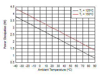
A common technique to calculate the maximum power dissipation that a device can withstand is by using the junction-to-ambient thermal resistance (RθJA), provided in the Thermal Information table. Using the equation power dissipation = (junction temperature, TJ – ambient temperature, TA) / RθJA, the amount of power a package can dissipate can be estimated. Figure 6-2 illustrates the package power dissipation based on this equation to reach junction temperatures of 125°C and 150°C at various ambient temperatures. The RθJA value is determined using industry standard JEDEC specifications and allows ease of comparing various packages. Power greater than that in Figure 6-2 can be dissipated in a package by good printed circuit board (PCB) thermal design, using heat sinks, and or active cooling techniques. See the Thermal Design By Insight, Not Hindsight application report for an in-depth discussion on thermal design.
 Figure 6-2 Package Power Dissipation vs Ambient Temperature