SBOS974F August 2019 – December 2024 THS6222
PRODUCTION DATA
- 1
- 1 Features
- 2 Applications
- 3 Description
- 4 Pin Configuration and Functions
- 5 Specifications
- 6 Detailed Description
- 7 Application and Implementation
- 8 Device and Documentation Support
- 9 Revision History
- 10Mechanical, Packaging, and Orderable Information
Package Options
Refer to the PDF data sheet for device specific package drawings
Mechanical Data (Package|Pins)
- RGT|16
- YS|0
- RHF|24
Thermal pad, mechanical data (Package|Pins)
- RGT|16
Orderable Information
6.3.1 Common-Mode Buffer
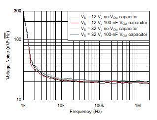
The THS6222 is a differential line driver that features an integrated common-mode buffer. Figure 7-2 shows that the most-common line-driving applications for the THS6222 are ac-coupled applications. Therefore, common-mode shift the inputs to confirm the input signals are within the common-mode specifications of the device. To maximize the dynamic range, the common-mode voltage is shifted to midsupply in most ac-coupled applications. With the integrated common-mode buffer, no external components are required to shift the input common-mode voltage. Engineers often choose to connect a noise-decoupling capacitor to the VCM pin. However, as shown in Figure 6-1, assuming the circuit is reasonably shielded from external noise sources, no difference in common-mode noise is observed with the 100‑nF capacitor or without the capacitor.
 Figure 6-1 Common-Mode Voltage Noise Density vs Frequency
There are ESD protection diodes in series directly at the output of the common-mode buffer between the internal 520‑Ω resistor and the common-mode buffer output. These diodes are referenced to midsupply. Any voltage that is 1.4 V greater or less than the midsupply applied to the VCM pin forward biases the protection diodes. This biasing results in either current flowing into or out of the VCM pin. The current is limited by the 520‑Ω resistor in series, but to prevent permanent damage to the device, limit the current to the specifications in the Absolute Maximum Ratings.