SBOS877A April   2018  – September 2018 THS6301

PRODUCTION DATA.  

  1. Features
  2. Applications
  3. Description
    1.     Device Images
      1.      MTPR G.Fast 212 MHz (Bias 10, PAR = 15 dB, 1-in-64 Missing Tones)
      2.      Multitone Power Ratio (MTPR) Profile (G.Fast, 212 MHz, 8 dBm)
  4. Revision History
  5. Pin Configuration and Functions
    1.     Pin Functions
  6. Specifications
    1. 6.1 Absolute Maximum Ratings
    2. 6.2 ESD Ratings
    3. 6.3 Recommended Operating Conditions
    4. 6.4 Thermal Information
    5. 6.5 Electrical Characteristics
    6. 6.6 Switching Characteristics
    7. 6.7 Typical Characteristics
  7. Detailed Description
    1. 7.1 Overview
    2. 7.2 Functional Block Diagram
    3. 7.3 Feature Description
    4. 7.4 Device Functional Modes
    5. 7.5 Programming
  8. Application and Implementation
    1. 8.1 Application Information
    2. 8.2 Typical Application
      1. 8.2.1 Design Requirements
      2. 8.2.2 Detailed Design Procedure
      3. 8.2.3 Application Curves
  9. Power Supply Recommendations
  10. 10Layout
    1. 10.1 Layout Guidelines
      1. 10.1.1 Power Dissipation and Thermal Considerations
    2. 10.2 Layout Example
  11. 11Device and Documentation Support
    1. 11.1 Documentation Support
      1. 11.1.1 Related Documentation
    2. 11.2 Receiving Notification of Documentation Updates
    3. 11.3 Community Resources
    4. 11.4 Trademarks
    5. 11.5 Electrostatic Discharge Caution
    6. 11.6 Glossary
  12. 12Mechanical, Packaging, and Orderable Information

Package Options

Mechanical Data (Package|Pins)
Thermal pad, mechanical data (Package|Pins)
Orderable Information

Typical Characteristics

at TA ≈ 25°C, VS+ = 12 V, VS– = 0 V, voltage gain (AV) = 8.5 V/V, 100-Ω load, RSERIES = 47.5 Ω, RIADJ = 75 kΩ, CIADJ = 100 pF, and drive mode 5 (B1B2 = 01, G.Fast mid power mode) and output power measured at input of transformer (1:1) with no assumed transformer insertion losses (unless otherwise noted)
THS6301 D001_SSBW.gif
VOUT = 1 VPP
Figure 1. Small-Signal Bandwidth
THS6301 D003_LSBW.gif
VOUT = 15 VPP
Figure 3. Large-Signal Bandwidth
THS6301 D005_Bias10_Distortion-vs-Frequency.gif
VOUT = 1 VPP
Figure 5. Distortion vs Frequency Drive Mode 6 (Bias 10)
THS6301 D007_Noise_TerminationModes.gif
Figure 7. Termination Mode Noise Floor
THS6301 D009_PulseResponse-SR_0Z.gif
SR down = 3200 V/µs, SR up = 2500 V/µs
Figure 9. Pulse Response Drive Mode 1 (Bias 0Z)
THS6301 D011_PulseResponse-SR_11.gif
SR down = 6400 V/µs, SR up = 4400 V/µs
Figure 11. Pulse Response Drive Mode 3 (Bias 11)
THS6301 D013_PulseResponse-SR_01.gif
SR down = 8200 V/µs, SR up = 6500 V/µs
Figure 13. Pulse Response Drive Mode 5 (Bias 01)
THS6301 D015_PulseResponse-SR_00-Z0-ZZ.gif
Figure 15. Pulse Response Termination and Power-Down Modes
THS6301 D021_MTPR_GFast212_10_OverTemp.gif
PAR = 15 dB, 1-in-64 missing tones, Line power = 8 dBm
Figure 17. MTPR Over Temperature G.Fast 212-MHz Profile (Bias 10)
THS6301 D023_MTPR_GFast106_10-01-1Z_4dBm.gif
PAR = 15 dB, 1-in-64 missing tones, line power = 4 dBm
Figure 19. MTPR G.Fast 106-MHz Profile
THS6301 D025_MTPR_VDSL35b_1Z-11-Z1_8dBm.gif
PAR = 15 dB, 1-in-64 missing tones, line power = 8 dBm
Figure 21. MTPR VDSL2-35b Profile
THS6301 D027_MTPR_VDSL17a_1Z-11-Z1_8dBm.gif
PAR = 15 dB, 1-in-4 missing tones, line power = 8 dBm
Figure 23. MTPR VDSL2-17a Profile
THS6301 D029_PowerConsumption_GFast106ProfileBiasModes.gif
G.Fast 106-MHz profile used
Figure 25. G.Fast Modes Power Consumption
THS6301 D033_ModeSwitchTiming_00-to-10.gif
Bias mode 00 to 10 and 10 to 00
Figure 27. Mode Switch Time 00 to 10
THS6301 D031_ModeSwitchTiming_ZZ-to-1Z.gif
Bias mode ZZ to 1Z and 1Z to ZZ
Figure 29. Mode Switch Time ZZ to 1Z
THS6301 D035_Iq-vs-Temp_10.gif
Figure 31. IQ vs Temperature Drive Mode 6 (Bias 10)
THS6301 D037_Iq-vs-Temp_1Z.gif
Figure 33. IQ vs Temperature Drive Mode 4 (Bias 1Z)
THS6301 D039_Iq-vs-Temp_Z1.gif
Figure 35. IQ vs Temperature Drive Mode 2 (Bias Z1)
THS6301 D041_Iq-vs-Temp_00.gif
Figure 37. IQ vs Temperature High-Power Termination Mode (Bias 00)
THS6301 D043_Iq-vs-Temp_ZZ.gif
Figure 39. IQ vs Temperature Power-Down Mode (Bias ZZ)
THS6301 D002_SSBW_3dB_Normalized.gif
VOUT = 1 VPP
Figure 2. 3-dB Normalized Gain Small-Signal Bandwidth
THS6301 D004_BiasModes_vs_Distortion.gif
Frequency = 50 MHz, VOUT = 1 VPP
Figure 4. Bias Modes vs Distortion
THS6301 D006_Noise_DriveModes.gif
Figure 6. Input Voltage Noise
THS6301 D008_Zout_TerminationModes.gif
Simulation data
Figure 8. Termination Mode Differential Output Impedance
THS6301 D010_PulseResponse-SR_Z1.gif
SR down = 4000 V/µs, SR up = 3200 V/µs
Figure 10. Pulse Response Drive Mode 2 (Bias Z1)
THS6301 D012_PulseResponse-SR_1Z.gif
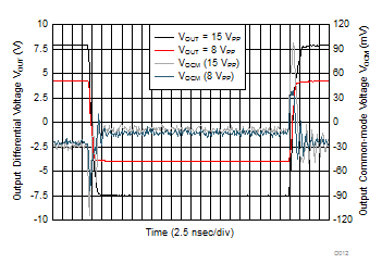
SR down = 7100 V/µs, SR up = 5400 V/µs
Figure 12. Pulse Response Drive Mode 4 (Bias 1Z)
THS6301 D014_PulseResponse-SR_10.gif
SR down = 10500 V/µs, SR up = 8000 V/µs
Figure 14. Pulse Response Drive Mode 6 (Bias 10)
THS6301 D020_MTPR_GFast212_10.gif
PAR = 15 dB, 1-in-64 missing tones
Figure 16. MTPR G.Fast 212-MHz Profile (Bias 10)
THS6301 D022_MTPR_GFast106_10-01-1Z_8dBm.gif
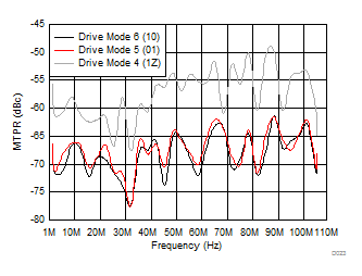
PAR = 15 dB, 1-in-64 missing tones, line power = 8 dBm
Figure 18. MTPR G.Fast 106-MHz Profile
THS6301 D024_MTPR_GFast106_01_8dBm_OverTemp.gif
Line power = 8 dBm, PAR = 15 dB, 1-in-64 missing tones
Figure 20. MTPR Over Temperature G.Fast 106-MHz Profile (Bias 01)
THS6301 D026_MTPR_VDSL30a_1Z-11-Z1_8dBm.gif
PAR = 15 dB, 1-in-4 missing tones, line power = 8 dBm
Figure 22. MTPR VDSL2-30a Profile
THS6301 D028_MTPR_ADSL2plus_0Z_8dBm.gif
PAR = 15 dB, 1-in-4 missing tones, line power = 8 dBm
Figure 24. MTPR ADSL2+ Profile
THS6301 D030_PowerConsumption_VDSL2-30aProfileBiasModes.gif
VDSL2-30a profile used
Figure 26. xDSL Modes Power Consumption
THS6301 D034_ModeSwitchTiming_ZZ-to-0Z.gif
Bias mode ZZ to 0Z and 0Z to ZZ
Figure 28. Mode Switch Time ZZ to 0Z
THS6301 D032_ModeSwitchTiming_Z0-to-Z1.gif
Bias mode Z0 to Z1and Z1 to Z0
Figure 30. Mode Switch Time Z0 to Z1
THS6301 D036_Iq-vs-Temp_01.gif
Figure 32. IQ vs Temperature Drive Mode 5 (Bias 01)
THS6301 D038_Iq-vs-Temp_11.gif
Figure 34. IQ vs Temperature Drive Mode 3 (Bias 11)
THS6301 D040_Iq-vs-Temp_0Z.gif
Figure 36. IQ vs Temperature Drive Mode 1 (Bias 0Z)
THS6301 D042_Iq-vs-Temp_Z0.gif
Figure 38. IQ vs Temperature Low-Power Termination Mode (Bias Z0)
THS6301 D044_VosHistogram.gif
Approximately 2100 units
Figure 40. Output Offset Voltage Histogram