SLOS932 December 2015 THS7530-Q1
PRODUCTION DATA.
- 1 Features
- 2 Applications
- 3 Description
- 4 Revision History
- 5 Pin Configuration and Functions
- 6 Specifications
- 7 Parameter Measurement Information
- 8 Detailed Description
- 9 Application and Implementation
- 10Power Supply Recommendations
- 11Layout
- 12Device and Documentation Support
- 13Mechanical, Packaging, and Orderable Information
Package Options
Mechanical Data (Package|Pins)
- PWP|14
Thermal pad, mechanical data (Package|Pins)
- PWP|14
Orderable Information
1 Features
- Qualified for Automotive Applications
- AEC-Q100 Qualified With the Following Results:
- Device Temperature Grade 1: –40°C to +125°C Ambient Operating Temperature Range
- Device HBM Classification Level 2
- Device CDM Classification Level C6
- Low Noise: Vn = 1.1 nV/√Hz,
Noise Figure = 9 dB - Low Distortion:
- HD2 = –65 dBc, HD3 = –61 dBc at 32 MHz
- IMD3 = –62 dBc, OIP3 = 21 dBm at 70 MHz
- 300-MHz Bandwidth
- Continuously Variable Gain Range: 11.6 dB
to 46.5 dB - Gain Slope: 38.8 dB/V
- Fully Differential Input and Output
- Output Common-Mode Voltage Control
- Output Voltage Limiting
2 Applications
- Time Gain Amplifiers in Ultra Sound, Sonar,
and Radar - Automatic Gain Control in Communication
and Video - System Gain Calibration in Communications
- Variable Gain in Instrumentation
3 Description
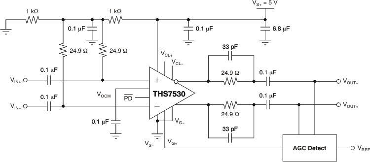
The THS7530-Q1 device is fabricated using Texas Instruments' state-of-the-art BiCom III SiGe complementary bipolar process. The THS7530-Q1 device is a DC-coupled, wide bandwidth amplifier with voltage-controlled gain. The amplifier has high-impedance differential inputs and low-impedance differential outputs with high-bandwidth gain control, output common-mode control, and output voltage clamping.
Signal-channel performance is exceptional with
300-MHz bandwidth, and third harmonic distortion of –61 dBc at 32 MHz with 1-VPP output into 400 Ω.
Gain control is linear in dB with 0 V to 0.9 V varying the gain from 11.6 dB to 46.5 dB with 38.8-dB/V gain slope.
Output voltage limiting is provided to limit the output voltage swing and to prevent saturating following stages.
The device is characterized for operation over the automotive temperature range, –40°C to +125°C.
Device Information(1)
| PART NUMBER | PACKAGE | BODY SIZE (NOM) |
|---|---|---|
| THS7530-Q1 | HTSSOP (14) | 5.00 mm × 4.40 mm |
- For all available packages, see the orderable addendum at the end of the data sheet.
