SLOS932 December 2015 THS7530-Q1
PRODUCTION DATA.
- 1 Features
- 2 Applications
- 3 Description
- 4 Revision History
- 5 Pin Configuration and Functions
- 6 Specifications
- 7 Parameter Measurement Information
- 8 Detailed Description
- 9 Application and Implementation
- 10Power Supply Recommendations
- 11Layout
- 12Device and Documentation Support
- 13Mechanical, Packaging, and Orderable Information
Package Options
Mechanical Data (Package|Pins)
- PWP|14
Thermal pad, mechanical data (Package|Pins)
- PWP|14
Orderable Information
9 Application and Implementation
NOTE
Information in the following applications sections is not part of the TI component specification, and TI does not warrant its accuracy or completeness. TI’s customers are responsible for determining suitability of components for their purposes. Customers should validate and test their design implementation to confirm system functionality.
9.1 Application Information
The THS7530-Q1 device is designed to work in a wide variety of applications requiring continuously variable gain and a fully-differential signal path. The common-mode voltage control and the output voltage clamps enable the THS7530-Q1 device to drive a diverse array of receiving circuits.
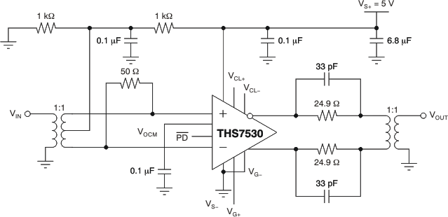 Figure 18. EVM Schematic: Designed for Use With Typical 50-Ω RF Test Equipment
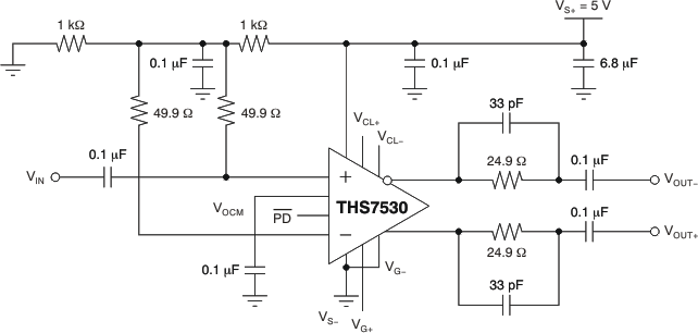
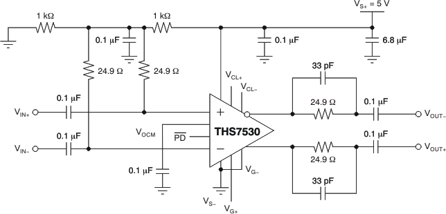 Figure 20. AC-Coupled Differential Input With AC-Coupled Differential Output
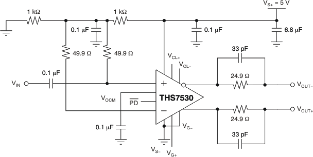 Figure 21. DC-Coupled Single-Ended Input With DC-Coupled Differential Output
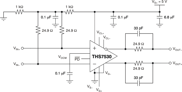 Figure 22. DC-Coupled Differential Input With DC-Coupled Differential Output
9.2 Typical Application
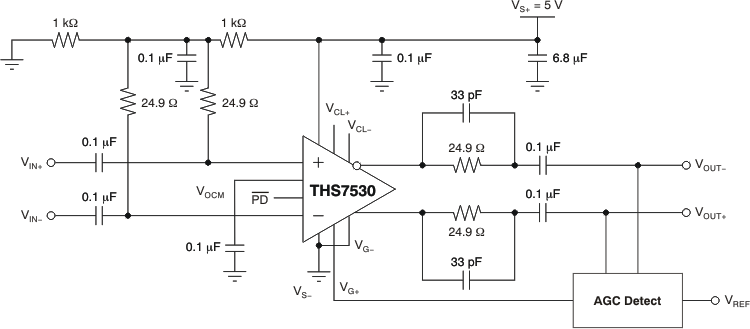 Figure 23. Typical Application Circuit
9.2.1 Design Requirements
A typical application circuit is shown in Figure 23. Two noteworthy aspects of this circuit are the customer’s automatic gain control (AGC) circuit and the THS7530-Q1 input bias circuit.
The proper design of the AGC circuit is essential for the THS7530-Q1 device to operate properly in the customer’s application. The method of detecting the amplitude of the differential output of the THS7530-Q1 device and creating the gain-control voltage, VG+, from the detected amplitude and the reference amplitude, Vref, are application-specific and beyond the scope of this document. The bandwidth of the amplitude of the THS7530-Q1 amplitude control is 15 MHz, which allows for rapid corrections of amplitude errors but which also allows noise from DC to 15 MHz to create an amplitude error. The trade-off between rapid amplitude correction and amplitude modulation due to noise is an important design consideration.
The input bias currents of the differential inputs of the THS7530-Q1 device are typically 20 µA. When the differential inputs are AC-coupled, the bias currents must be supplied as shown in Figure 23. In this circuit, the DC bias voltage is mid-supply and the AC differential input impedance is 50 Ω. The 0.1-µF capacitor between the two 24.9-Ω resistors creates an AC ground for the driving circuit.
9.2.2 Detailed Design Procedure
The THS7530-Q1 device is designed for nominal 5-V power supply from VS+ to VS–.
The amplifier has fully differential inputs, VIN+ and VIN–, and fully differential outputs, VOUT+ and VOUT– The inputs are high impedance and outputs are low impedance. External resistors are recommended for impedance matching and termination purposes.
The inputs and outputs can be DC-coupled, but for best performance, the input and output common-mode voltage should be maintained at the midpoint between the two supply pins. The output common-mode voltage is controlled by the voltage applied to VOCM. Left unterminated, VOCM is set to midsupply by internal resistors. A 0.1-µF bypass capacitor should be placed between VOCM and ground to reduce common-mode noise. The input common-mode voltage defaults to midrail when left unconnected. For voltages other than midrail, VOCMmust be biased by external means. VIN+ and VIN– both require a nominal 30-µA bias current for proper operation. Therefore, ensure equal input impedance at each input to avoid generating an offset voltage that varies with gain.
Voltage applied from VG– to VG+ controls the gain of the part with 38.8-dB/V gain slope. The input can be differential or single ended. VG– must be maintained within –0.6 V and 0.8 V of VS–for proper operation. The negative gain input should typically be tied directly to the negative power supply.
VCL+ and VCL– are inputs that limit the output voltage swing of the amplifier. The voltages applied set an absolute limit on the voltages at the output. Input voltages at VCL+ and VCL– clamp the output, ensuring that neither output exceeds those values.
The power-down input is a TTL compatible input, referenced to the negative supply voltage. A logic low puts the THS7530-Q1 device in power-saving mode. In power-down mode the part consumes less than 1-mA current, the output goes high impedance, and a high amount of isolation is maintained between the input and output.
Power-supply bypass capacitors are required for proper operation. A 6.8-µF tantalum bulk capacitor is recommended if the amplifier is located far from the power supply and may be shared among other devices. A ceramic 0.1-µF capacitor is recommended within 0.1-in of the device power pin. The ceramic capacitors should be located on the same layer as the amplifier to eliminate the use of vias between the capacitors and the power pin.
Table 2. THS7530EVM Bill of Materials
| ITEM NO. | DESCRIPTION | SIZE | REFERENCE DESIGNATOR | QTY | PART NUMBER |
|---|---|---|---|---|---|
| 1 | Bead, ferrite, 3 A, 80 Ω | 1206 | FB1 | 1 | (Steward) HI1206N800R–00 |
| 2 | Capacitor, tantalum, 6.8 mF, 35 V, 10% | D | C2 | 1 | (AVX) TAJD685K035R |
| 3 | Capacitor, ceramic, 0.1 mF, X7R, 16V | 508 | C1 | 1 | (AVX) 0508YC104KAT2A |
| 5 | Capacitor, ceramic, 0.1 mF, X7R, 50 V | 805 | C3, C7, C12, C13, C14, C15, C16, C17 | 8 | (AVX) 08055C104KAT2A |
| 6 | Diode, Schottky, 20 V, 0.5 A | SOD-123 | D1 | 1 | (Diodes Inc.) B0520LW–7 |
| 7 | Resistor, 10 Ω, 1/8 W, 1% | 805 | R24, R25, R26 | 3 | (PHYCOMP) 9C08052A10R0FKHFT |
| 8 | Resistor, 24.9 Ω, 1/8 W, 1% | 805 | R9, R15 | 2 | (PHYCOMP) 9C08052A24R9FKHFT |
| 9 | Resistor, 1 kΩ, 1.8W, 1% | 805 | R7, R12 | 2 | (PHYCOMP) 9C08052A1001FKHFT |
| 10 | Resistor, 3.92 kΩ , 1/8 W, 1% | 805 | R1 | 1 | (PHYCOMP) 9C08052A3921FKHFT |
| 11 | Resistor, 0 Ω, 1/4 W | 1206 | C4, C5 | 2 | (PHYCOMP) 9C12063A0R00JLHFT |
| 12 | Resistor, 49.9 Ω, 1/4 W, 1% | 1206 | R4 | 1 | (PHYCOMP) 9C12063A49R9FKRFT |
| 13 | Pot., ceramic, 1/4 inch square, 1 kΩ | R2 | 1 | (Bourns) 3362P–1–102 | |
| 14 | Pot., ceramic, 1/4 inch square, 10 kΩ | R21, R22, R23 | 3 | (Bourns) 3362P–1–103 | |
| 15 | IC, TLV2371 | SOT-23 | U2, U3, U4 | 3 | (TI) TLV2371IDBVT |
| 16 | Transformer, 1:1 | CD542 | T1, T2 | 2 | (Mini-Circuits) ADT1-1WT |
| 17 | Connector, edge, SMA PCB Jack | J3, J4 | 2 | (Johnson) 142–0701–801 | |
| 18 | Jack, banana receptacle, 0.25-in diameter hole | J1, J2 | 2 | (HH Smith) 101 | |
| 19 | Header, 0.1-in Ctrs, 0.025-in square pins | 2 POS. | JP1 | 1 | (Sullins) PZC36SAAN |
| 20 | Shunts | JP1 | 1 | (Sullins) SSC02SYAN | |
| 21 | Test point, black | TP2, TP3, TP4 | 3 | (Keystone) 5001 | |
| 22 | Test points, red | TP1, TP8, TP9, TP10 | 4 | (Keystone) 5000 | |
| 23 | Standoff, 4–40 Hex, 0.625-in Length | 4 | (Keystone) 1804 | ||
| 24 | Screw, Phillips, 4–40, .250-in | 4 | SHR–0440–016–SN | ||
| 25 | IC, THS7530-Q1 | U1 | 1 | (TI) THS7530QPWPRQ1 | |
| 26 | Board, printed circuit | 1 | (TI) EDGE # 6441987 |
