SLOS932 December 2015 THS7530-Q1
PRODUCTION DATA.
- 1 Features
- 2 Applications
- 3 Description
- 4 Revision History
- 5 Pin Configuration and Functions
- 6 Specifications
- 7 Parameter Measurement Information
- 8 Detailed Description
- 9 Application and Implementation
- 10Power Supply Recommendations
- 11Layout
- 12Device and Documentation Support
- 13Mechanical, Packaging, and Orderable Information
Package Options
Mechanical Data (Package|Pins)
- PWP|14
Thermal pad, mechanical data (Package|Pins)
- PWP|14
Orderable Information
6 Specifications
6.1 Absolute Maximum Ratings
Over operating free-air temperature range, unless otherwise noted.(1)| MIN | MAX | UNIT | |||
|---|---|---|---|---|---|
| VS+ – VS– | Supply voltage | 5.5 | V | ||
| VI | Input voltage | ±VS | V | ||
| IO | Output current | 65 | mA | ||
| VID | Differential input voltage | ±4 | V | ||
| Continuous power dissipation | See Thermal Information | ||||
| TJ | Maximum junction temperature | 150 | °C | ||
| Maximum junction temperature for long term stability(2) | 125 | °C | |||
| Tstg | Storage temperature | –65 | 150 | °C | |
(1) Stresses beyond those listed under Absolute Maximum Ratings may cause permanent damage to the device. These are stress ratings only, which do not imply functional operation of the device at these or any other conditions beyond those indicated under Recommended Operating Conditions. Exposure to absolute-maximum-rated conditions for extended periods may affect device reliability.
(2) The maximum junction temperature for continuous operation is limited by package constraints. Operation above this temperature may result in reduced reliability and/or lifetime of the device.
6.2 ESD Ratings
| VALUE | UNIT | |||
|---|---|---|---|---|
| V(ESD) | Electrostatic discharge | Human-body model (HBM), per AEC Q100-002(1) | ±2000 | V |
| Charged-device model (CDM), per AEC Q100-011 | ±1000 | |||
(1) AEC Q100-002 indicates that HBM stressing shall be in accordance with the ANSI/ESDA/JEDEC JS-001 specification.
6.3 Recommended Operating Conditions
| MIN | NOM | MAX | UNIT | |||
|---|---|---|---|---|---|---|
| [VS– to VS+] | Supply voltage | 4.5 | 5 | 5.5 | V | |
| Input common mode voltage | [VS– to VS+] = 5 V | 2.5 | V | |||
| Output common mode voltage | [VS– to VS+] = 5 V | 2.5 | V | |||
| TA | Operating free-air temperature | –40 | 125 | °C | ||
6.4 Thermal Information
| THERMAL METRIC(1) | THS7530 | UNIT | |
|---|---|---|---|
| PWP (HTSSOP) | |||
| 14 PINS | |||
| RθJA | Junction-to-ambient thermal resistance | 75.3 | °C/W |
| RθJC(top) | Junction-to-case (top) thermal resistance | 35 | °C/W |
| RθJB | Junction-to-board thermal resistance | 28.9 | °C/W |
| ψJT | Junction-to-top characterization parameter | 1.6 | °C/W |
| ψJB | Junction-to-board characterization parameter | 28.6 | °C/W |
| RθJC(bot) | Junction-to-case (bottom) thermal resistance | 3.2 | °C/W |
(1) For more information about traditional and new thermal metrics, see the Semiconductor and IC Package Thermal Metrics application report, SPRA953.
6.5 Electrical Characteristics: Main Amplifier
VS+ = 5 V, VS– = 0 V, VOCM = 2.5 V, VICM = 2.5 V, VG- = 0 V, VG+ = 1 V (maximum gain), TA = 25°C, AC performance measured using the AC test circuit shown in Figure 16 (unless otherwise noted). DC performance is measured using the DC test circuit shown in Figure 17 (unless otherwise noted)| PARAMETER | TEST CONDITIONS | MIN | TYP | MAX | UNIT | |
|---|---|---|---|---|---|---|
| AC PERFORMANCE | ||||||
| Small-signal bandwidth | All gains, PIN = –45 dBm | 300 | MHz | |||
| Slew rate(1) | 1-VPP Step, 25% to 75%, minimum gain | 1250 | V/µs | |||
| Settling time to 1%(1) | 1-VPP Step, minimum gain | 11 | ns | |||
| Harmonic distortion, 2nd harmonic | f = 32 MHz, VO(PP) = 1 V, RL(diff)= 400 Ω | –65 | dBc | |||
| Harmonic distortion, 3rd harmonic | f = 32 MHz, VO(PP) = 1 V, RL(diff)= 400 Ω | –61 | dBc | |||
| Third-order intermodulation distortion | PO = –10 dBm each tone, fC= 70 MHz, 200-kHz tone spacing |
–62 | dBc | |||
| Third-order output intercept point | fC= 70 MHz, 200-kHz tone spacing | 21 | dBm | |||
| Noise figure (with input termination) | Source impedance: 50 Ω | 9 | dB | |||
| Total input voltage noise | f > 100 kHz | 1.1 | nV/√Hz | |||
| DC PERFORMANCE—INPUTS | ||||||
| Input bias current | TA = 25°C | 20 | 39 | µA | ||
| TA = –40°C to +125°C | 40 | |||||
| Input bias current offset | <150 | pA | ||||
| Minimum input voltage | Minimum gain, TA = 25°C | 1.5 | 1.6 | V | ||
| Minimum gain, TA = –40°C to +125°C | 1.7 | |||||
| Maximum input voltage | Minimum gain, TA = 25°C | 3.2 | 3.3 | V | ||
| Minimum gain, TA = –40°C to +125°C | 3.15 | |||||
| Common-mode rejection ratio | TA = 25°C | 56 | 114 | dB | ||
| TA = –40°C to +125°C | 44 | |||||
| Differential input impedance | 8.5 || 3 | kΩ || pF | ||||
| DC PERFORMANCE—OUTPUTS | ||||||
| Output offset voltage | All gains, TA = 25°C | ±100 | ±410 | mV | ||
| All gains, TA = –40°C to +125°C | ±480 | |||||
| Maximum output voltage high | TA = 25°C | 3.25 | 3.5 | V | ||
| TA = –40°C to +125°C | 3 | |||||
| Minimum output voltage low | TA = 25°C | 1.5 | 1.8 | V | ||
| TA = –40°C to +125°C | 2 | |||||
| Output current | TA = 25°C | ±16 | ±30 | mA | ||
| TA = –40°C to +125°C | ±16 | |||||
| Output impedance | 15 | Ω | ||||
| OUTPUT COMMON-MODE VOLTAGE CONTROL | ||||||
| Small-signal bandwidth | 32 | MHz | ||||
| Gain | 1 | V/V | ||||
| Common-mode offset voltage | TA = 25°C | 4.5 | 12 | mV | ||
| TA = –40°C to +125°C | 13.8 | |||||
| Minimum input voltage | 1.75 | V | ||||
| Maximum input voltage | 3.25 | V | ||||
| Input impedance | 25 || 1 | kΩ || pF | ||||
| Default voltage, with no connect | 2.5 | V | ||||
| Input bias current | <1 | µA | ||||
| GAIN CONTROL | ||||||
| Gain control differential voltage range | VG+ | 0 to 1 | V | |||
| Minus gain control voltage | VG– – VS– | –0.6 to 0.8 | V | |||
| Minimum gain | VG+ = 0 V | 11.6 | dB | |||
| Maximum gain | VG+ = 0.9 V | 46.5 | dB | |||
| Gain slope | VG+ = 0 V to 0.9 V | 38.8 | dB/V | |||
| Gain slope variation | VG+ = 0 V to 0.9 V | ±1.5 | dB/V | |||
| Gain error | VG+ = 0 V to 0.15 V | ±4 | dB | |||
| VG+ = 0.15 V to 0.9 V | ±2.25 | |||||
| Gain control input bias current | <1 | µA | ||||
| Gain control input resistance | 40 | kΩ | ||||
| Gain control bandwidth | Small signal –3 dB | 15 | MHz | |||
| VOLTAGE CLAMPING | ||||||
| Output voltages (VOUT±) relative to clamp voltages (VCL±) | Device In voltage limiting mode, TA = 25°C | ±25 | ±40 | mV | ||
| Device In voltage limiting mode, TA = –40°C to +125°C | ±180 | |||||
| Clamp voltage (VCL±) input resistance | Device in voltage limiting mode | 3.3 | kΩ | |||
| Clamp voltage (VCL±) limits | VS– to VS+ | V | ||||
| POWER SUPPLY | ||||||
| Specified operating voltage | TA = 25°C | 5 | 5.5 | V | ||
| TA = –40°C to +125°C | 5.5 | |||||
| Maximum quiescent current | TA = 25°C | 40 | 48 | mA | ||
| TA = –40°C to +125°C | 49 | |||||
| Power supply rejection (±PSRR) | TA = 25°C | 70 | 77 | dB | ||
| TA = –40°C to +125°C | 45 | |||||
| POWER DOWN | ||||||
| Enable voltage threshold | TTL low = shut down, TA = 25°C | 1.4 | V | |||
| TTL low = shut down, TA = –40°C to +125°C |
1 | |||||
| Disable voltage threshold | TTL high = normal operation, TA = 25°C | 1.4 | V | |||
| TTL high = normal operation, TA = –40°C to +125°C |
1.65 | |||||
| Power-down quiescent current | TA = 25°C | 0.35 | 0.4 | mA | ||
| TA = –40°C to +125°C | 0.55 | |||||
| Input current high | TA = 25°C | ±9 | ±16 | µA | ||
| TA = –40°C to +125°C | ±19 | |||||
| Input current low | TA = 25°C | ±109 | ±116 | µA | ||
| TA = –40°C to +125°C | ±130 | |||||
| Input impedance | 50 || 1 | kΩ || pF | ||||
| Turnon time delay | Measured to 50% quiescent current | 820 | ns | |||
| Turnoff time delay | Measured to 50% quiescent current | 500 | ns | |||
| Forward isolation in power down | 80 | dB | ||||
| Input resistance in power down | > 1 | MΩ | ||||
| Output resistance in power down | 16 | kΩ | ||||
(1) Slew rate and settling time measured at amplifier output.
6.6 Package Thermal Data
| PACKAGE | PCB | TA = 25°C POWER RATING(1) |
|---|---|---|
| PWP (14-pin)(2) | See Layout. | 3 W |
(1) This data was taken using 2 oz trace and copper pad that is soldered directly to a 3 in × 3 in PCB.
(2) The THS7530-Q1 incorporates a PowerPAD on the underside of the chip. The PowerpAD acts as a heatsink and must be connected to a thermally dissipative plane for proper power dissipation. Failure to do so may result in exceeding the maximum junction temperature which could permanently damage the device. See TI technical briefs SLMA002 and SLMA004 for more information about using the PowerPAD thermally enhanced package.
6.7 Typical Characteristics
Measured using the AC test circuit shown in Figure 16 (unless otherwise noted).Table 1. Table Of Graphs
| FIGURE | ||
|---|---|---|
| Voltage Gain to Load | vs Frequency (Input at 45 dBm) | Figure 1 |
| Gain and Gain Error | vs VG+ | Figure 2 |
| Noise Figure | vs Frequency | Figure 3 |
| Output Intercept Point | vs Frequency | Figure 4 |
| 1-dB Compression Point | vs Frequency | Figure 5 |
| Total Input Voltage Noise | vs Frequency | Figure 6 |
| Intermodulation Distortion | vs Frequency | Figure 7 |
| Harmonic Distortion | vs Frequency | Figure 8 |
| S-Parameters | vs Frequency | Figure 24 |
| Differential Input Impedance of Main Amplifier | vs Frequency | Figure 25 |
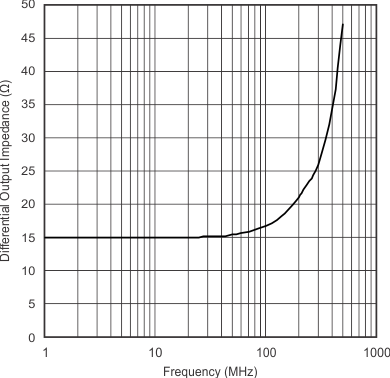
| Differential Output Impedance of Main Amplifier | vs Frequency | Figure 9 |
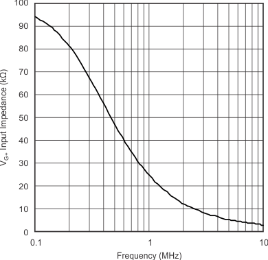
| VG+ Input Impedance | vs Frequency | Figure 10 |
| VOCM Input Impedance | vs Frequency | Figure 11 |
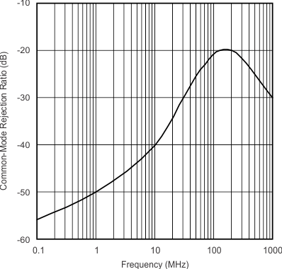
| Common-Mode Rejection Ratio | vs Frequency | Figure 12 |
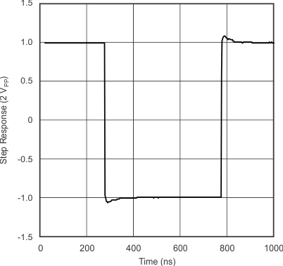
| Step Response: 2 VPP | vs Time | Figure 13 |
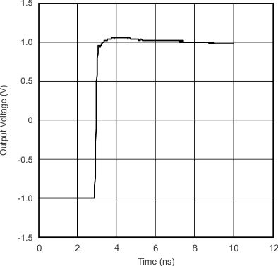
| Step Response: Rising Edge | vs Time | Figure 14 |
| Step Response: Falling Edge | vs Time | Figure 15 |
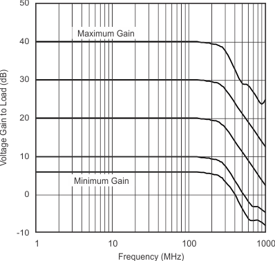
| Gain is taken at load. | Add 6 dB to refer to amplifier output | |
| PIN = –45 dBm | ||
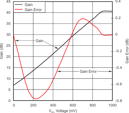
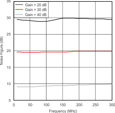
| Terminated input |
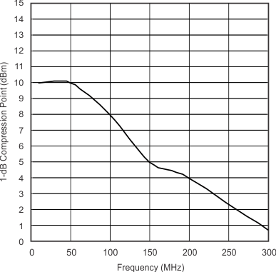
| Taken at load. | Add 3 dB to refer to amplifier output. | |
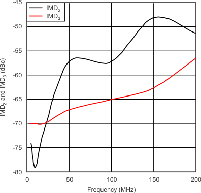
| VG+ = 1 V | VO = 1 VPP (composite) | RL = 400 Ω |
vs Frequency
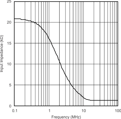
| RL = 400 Ω | At amplifier output and minimum gain | |
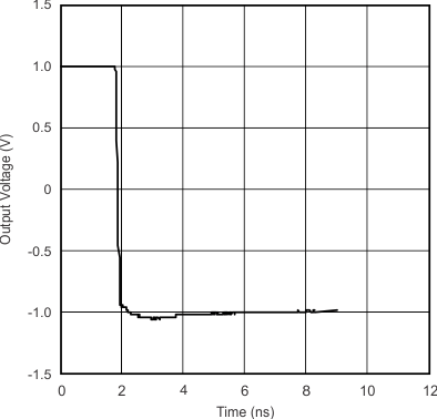
| RL = 400 Ω | At amplifier output and minimum gain | ||
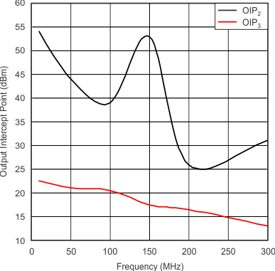
| Taken at load. | Add 3 dB to refer to amplifier output. | |
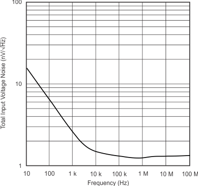
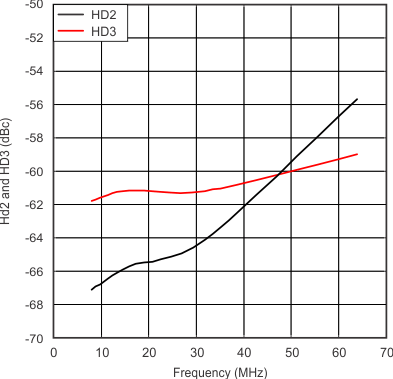
| VG+ = 1 V | VO = 1 VPP | RL = 400 Ω |
| RL = 400 Ω | At amplifier output and minimum gain | |