SLLSFN8 September 2023 THVD1330
PRODUCTION DATA
- 1
- 1 Features
- 2 Applications
- 3 Description
- 4 Revision History
- 5 Pin Configuration and Functions
- 6 Specifications
- 7 Parameter Measurement Information
- 8 Detailed Description
- 9 Application and Implementation
- 10Device and Documentation Support
- 11Mechanical, Packaging, and Orderable Information
Package Options
Mechanical Data (Package|Pins)
- D|8
Thermal pad, mechanical data (Package|Pins)
Orderable Information
7 Parameter Measurement Information
 Figure 7-1 Measurement of Driver
Differential Output Voltage With Common-Mode Load
 Figure 7-2 Measurement of Driver
Differential and Common-Mode Output With RS-485 Load
Generator: PRR =
500 kHz, 50% Duty Cycle, tr < 60 ns, tf < 6 ns
ZO = 50 Ω
Figure 7-3 Driver
Switching Test Circuit and Voltage Waveforms
Generator: PRR =
500 kHz, 50% Duty Cycle, tr < 60 ns, tf < 6 ns
ZO = 50 Ω
Figure 7-4 Driver
High-Level Enable and Disable Time Test Circuit and Voltage Waveforms
Generator: PRR =
500 kHz, 50% Duty Cycle, tr < 60 ns, tf < 6 ns
ZO = 50 Ω
Figure 7-5 Driver
Low-Level Output Enable and Disable Time Test Circuit and Voltage
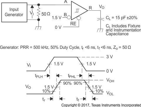
Waveforms Figure 7-6 Receiver
Switching Test Circuit and Voltage Waveforms
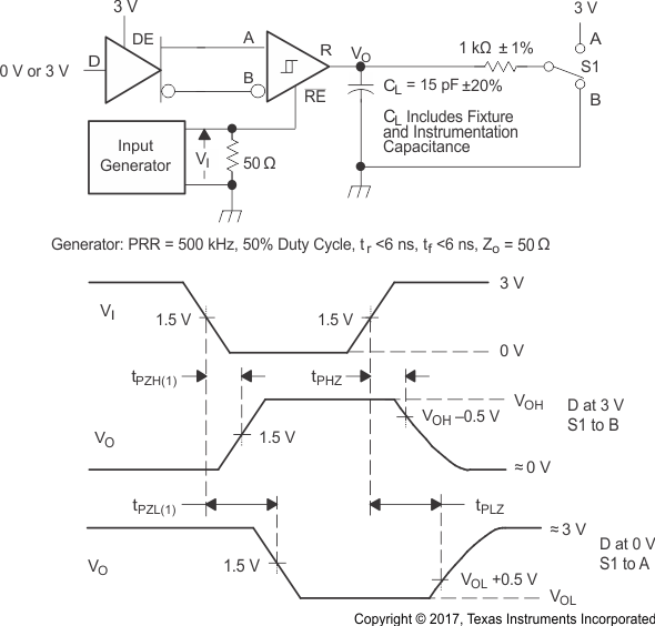
 Figure 7-7 Receiver
Enable and Disable Time Test Circuit and Voltage Waveforms With Drivers
Enabled
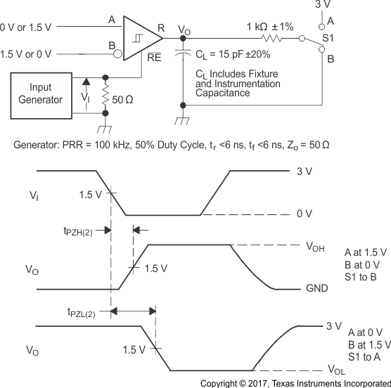
 Figure 7-8 Receiver
Enable Time From Standby (Driver Disabled)