SLLSF87A May   2021  – November 2021 THVD1406 , THVD1426

PRODUCTION DATA  

  1. Features
  2. Applications
  3. Description
  4. Revision History
  5. Pin Configuration and Functions
  6. Specifications
    1. 6.1  Absolute Maximum Ratings
    2. 6.2  ESD Ratings
    3. 6.3  ESD Ratings - IEC Specifications
    4. 6.4  Recommended Operating Conditions
    5. 6.5  Thermal Information
    6. 6.6  Power Dissipation Characteristics
    7. 6.7  Electrical Characteristics
    8. 6.8  Switching Characteristics (THVD1406)
    9. 6.9  Switching Characteristics (THVD1426)
    10. 6.10 Typical Characteristics
  7. Parameter Measurement Information
  8. Detailed Description
    1. 8.1 Overview
    2. 8.2 Functional Block Diagrams
    3. 8.3 Feature Description
    4. 8.4 Device Functional Modes
  9. Application Information Disclaimer
    1. 9.1 Application Information
    2. 9.2 Typical Application
      1. 9.2.1 Design Requirements
        1. 9.2.1.1 Data Rate and Bus Length
        2. 9.2.1.2 Stub Length
        3. 9.2.1.3 Bus Loading
        4. 9.2.1.4 Receiver Failsafe
        5. 9.2.1.5 Transient Protection
      2. 9.2.2 Detailed Design Procedure
      3. 9.2.3 Application Curves
  10. 10Power Supply Recommendations
  11. 11Layout
    1. 11.1 Layout Guidelines
    2. 11.2 Layout Example
  12. 12Device and Documentation Support
    1. 12.1 Device Support
      1. 12.1.1 Third-Party Products Disclaimer
    2. 12.2 Receiving Notification of Documentation Updates
    3. 12.3 Support Resources
    4. 12.4 Trademarks
    5. 12.5 Electrostatic Discharge Caution
    6. 12.6 Glossary
  13. 13Mechanical, Packaging, and Orderable Information

Package Options

Mechanical Data (Package|Pins)
Thermal pad, mechanical data (Package|Pins)
Orderable Information

Typical Characteristics

GUID-20201218-CA0I-1C1K-1HPW-KXS6GKSHZDLH-low.gif
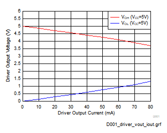
DE = VCC TA = 25°C
Figure 6-1 Driver Output voltage vs Driver Output Current
GUID-20201218-CA0I-BSJV-MXKW-BKS9TZVQFJF7-low.gif
RL = 54 Ω DE = VCC D = VCC
TA = 25°C
Figure 6-3 Driver Output Current vs Supply Voltage
GUID-20201218-CA0I-Z5W0-KT7D-HLBMXHPS6DCJ-low.gif
RL = 54 Ω CL = 50 pF
Figure 6-5 Driver Propagation Delay vs Temperature (THVD1406)
RL = 54 Ω CL = 50 pF
Figure 6-7 Driver Rise or Fall Time vs Temperature (THVD1426)
RL = 54 Ω TA = 25°C
Figure 6-9 Supply Current vs Signal Rate (THVD1426)
GUID-20201218-CA0I-FHSQ-SJFP-FZPPJ6HGPP4V-low.gif
D = 0 V DE = VCC TA = 25°C
Figure 6-2 Driver Differential Output voltage vs Driver Output Current
GUID-20201218-CA0I-GRFT-7KTS-FV3SC5BRXRPJ-low.gif
RL = 54 Ω CL = 50 pF
Figure 6-4 Driver Rise or Fall Time vs Temperature (THVD1406)
GUID-20201218-CA0I-BFRD-FZBZ-JRRDSRRVS0QR-low.gif
RL = 54 Ω TA = 25°C
Figure 6-6 Supply Current vs Signal Rate (THVD1406)
RL = 54 Ω CL = 50 pF
Figure 6-8 Driver Propagation Delay vs Temperature (THVD1426)