SLLSFS6A September 2024 – December 2024 TIOL221
PRODMIX
- 1
- 1 Features
- 2 Applications
- 3 Description
- 4 Pin Configuration and Functions
- 5 Specifications
- 6 Parameter Measurement Information
-
7 Detailed Description
- 7.1 Overview
- 7.2 Functional Block Diagrams
- 7.3
Feature Description
- 7.3.1 Wake-Up Detection
- 7.3.2 Current Limit Configuration
- 7.3.3 CQ Current Fault Detection, Indication and Auto Recovery
- 7.3.4 DO Current Fault Detection, Indication and Auto Recovery
- 7.3.5 CQ and DI Receivers
- 7.3.6 Fault Reporting
- 7.3.7 The Integrated Voltage Regulator (LDO)
- 7.3.8 Reverse Polarity Protection
- 7.3.9 Integrated Surge Protection and Transient Waveform Tolerance
- 7.3.10 Undervoltage Lock-Out (UVLO)
- 7.3.11 Interrupt Function
- 7.4 Device Functional Modes
- 7.5 SPI Programming
- 8 Application and Implementation
- 9 TIOL221 Registers
- 10Device and Documentation Support
- 11Revision History
- 12Mechanical, Packaging, and Orderable Information
Package Options
Refer to the PDF data sheet for device specific package drawings
Mechanical Data (Package|Pins)
- RGE|24
Thermal pad, mechanical data (Package|Pins)
Orderable Information
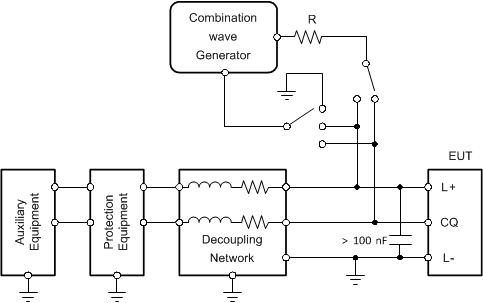
7.3.9 Integrated Surge Protection and Transient Waveform Tolerance
The LP, CQ, DO and DI pins of the device are capable of withstanding up to 1.2kV of 1.2/50 – 8/20μs IEC 61000-4-5 surge with a source impedance of 500Ω. The surge testing should be performed with a minimum 100nF supply decoupling capacitor between LP and LM, and 1µF between VOUT and LM.
External TVS diodes may be required for higher transient protection levels. The system designer must make sure the maximum clamping voltage of the external diodes is < 65V at the desired current level. The device is capable of withstanding up to ±70V transient pulses < 100µs.

1.2/50 – 8/20µs CWG
R = 500Ω
Figure 7-4 Surge Test Setup