SLOS080V september 1978 – april 2023 TL071 , TL071A , TL071B , TL071H , TL072 , TL072A , TL072B , TL072H , TL072M , TL074 , TL074A , TL074B , TL074H , TL074M
PRODUCTION DATA
- 1 Features
- 2 Applications
- 3 Description
- 4 Revision History
- 5 Pin Configuration and Functions
-
6 Specifications
- 6.1 Absolute Maximum Ratings
- 6.2 ESD Ratings
- 6.3 Recommended Operating Conditions
- 6.4 Thermal Information for Single Channel
- 6.5 Thermal Information for Dual Channel
- 6.6 Thermal Information for Quad Channel
- 6.7 Electrical Characteristics: TL07xH
- 6.8 Electrical Characteristics (DC): TL07xC, TL07xAC, TL07xBC, TL07xI, TL07xM
- 6.9 Electrical Characteristics (AC): TL07xC, TL07xAC, TL07xBC, TL07xI, TL07xM
- 6.10 Typical Characteristics: TL07xH
- 6.11 Typical Characteristics: All Devices Except TL07xH
- 7 Parameter Measurement Information
- 8 Detailed Description
- 9 Application and Implementation
- 10Device and Documentation Support
- 11Mechanical, Packaging, and Orderable Information
Package Options
Mechanical Data (Package|Pins)
Thermal pad, mechanical data (Package|Pins)
Orderable Information
6.11 Typical Characteristics: All Devices Except TL07xH

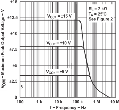
 Figure 6-42 Maximum Peak Output Voltage vs Frequency
 Figure 6-44 Maximum Peak Output Voltage vs Free-Air Temperature
 Figure 6-46 Maximum Peak Output Voltage vs Supply Voltage
 Figure 6-48 Large-Signal Differential Voltage Amplification and Phase Shift vs Frequency
 Figure 6-50 Common-Mode Rejection Ratio vs Free-Air Temperature
 Figure 6-52 Supply Current Per Amplifier vs Free-Air Temperature

 Figure 6-58 Output Voltage vs Elapsed Time
 Figure 6-43 Maximum Peak Output Voltage vs Frequency
 Figure 6-45 Maximum Peak Output Voltage vs Load Resistance
 Figure 6-47 Large-Signal Differential Voltage Amplification vs Free-Air Temperature
 Figure 6-49 Normalized Unity-Gain Bandwidth and Phase Shift vs Free-Air Temperature
 Figure 6-51 Supply Current Per Amplifier vs Supply Voltage
 Figure 6-53 Total Power Dissipation vs Free-Air Temperature

 Figure 6-59 VIO vs VCM