SLOS081N February 1977 – June 2024 TL081 , TL081A , TL081B , TL081H , TL082 , TL082A , TL082B , TL082H , TL084 , TL084A , TL084B , TL084H
PRODUCTION DATA
- 1
- 1 Features
- 2 Applications
- 3 Description
- 4 Pin Configuration and Functions
-
5 Specifications
- 5.1 Absolute Maximum Ratings
- 5.2 ESD Ratings
- 5.3 Recommended Operating Conditions
- 5.4 Thermal Information for Single Channel
- 5.5 Thermal Information for Dual Channel
- 5.6 Thermal Information for Quad Channel
- 5.7 Electrical Characteristics: TL08xH
- 5.8 Electrical Characteristics (DC): TL08xC, TL08xAC, TL08xBC, TL08xI, TL08xM
- 5.9 Electrical Characteristics (AC): TL08xC, TL08xAC, TL08xBC, TL08xI, TL08xM
- 5.10 Typical Characteristics: TL08xH
- 6 Parameter Measurement Information
- 7 Detailed Description
- 8 Applications and Implementation
- 9 Device and Documentation Support
- 10Revision History
- 11Mechanical, Packaging, and Orderable Information
Package Options
Refer to the PDF data sheet for device specific package drawings
Mechanical Data (Package|Pins)
- J|14
- FK|20
Thermal pad, mechanical data (Package|Pins)
Orderable Information
4 Pin Configuration and Functions
 Figure 4-1 TL081H DBV Package,
5-Pin SOT-23
(Top View)

NC- no
internal connection
Figure 4-3 TL081H D Package,8-Pin SOIC
(Top View)
 Figure 4-2 TL081H DCK
Package,
Figure 4-2 TL081H DCK
Package,5-Pin SC70
(Top View)
Table 4-1 Pin Functions: TL081H
| PIN | TYPE(1) | DESCRIPTION | |||
|---|---|---|---|---|---|
| NAME | DBV | DCK | D | ||
| IN– | 4 | 3 | 2 | I | Inverting input |
| IN+ | 3 | 1 | 3 | I | Noninverting input |
| NC | — | — | 8 | — | Do not connect |
| NC | — | — | 1 | — | Do not connect |
| NC | — | — | 5 | — | Do not connect |
| OUT | 1 | 4 | 6 | O | Output |
| VCC– | 2 | 2 | 4 | — | Power supply |
| VCC+ | 5 | 5 | 7 | — | Power supply |
(1) I = input, O = output
NC- no internal connection
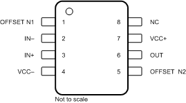
Figure 4-4 TL081x D, P, and PS Package,8-Pin SOIC, PDIP, and SO
(Top View)
Table 4-2 Pin Functions: TL081x
| PIN | TYPE(1) | DESCRIPTION | |
|---|---|---|---|
| NAME | NO. | ||
| IN– | 2 | I | Inverting input |
| IN+ | 3 | I | Noninverting input |
| NC | 8 | — | Do not connect |
| OFFSET N1 | 1 | — | Input offset adjustment |
| OFFSET N2 | 5 | — | Input offset adjustment |
| OUT | 6 | O | Output |
| VCC– | 4 | — | Power supply |
| VCC+ | 7 | — | Power supply |
(1) I = input, O = output
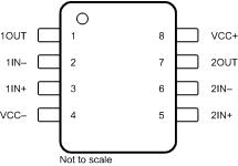 Figure 4-5 TL082x D, DDF, DGK, JG, P, PS, and PW Package,
8-Pin SOIC, SOT-23 (8), VSSOP, CDIP, PDIP, SO, and TSSOP
(Top View)
Table 4-3 Pin Functions: TL082x
| PIN | TYPE(1) | DESCRIPTION | |
|---|---|---|---|
| NAME | NO. | ||
| 1IN– | 2 | I | Inverting input |
| 1IN+ | 3 | I | Noninverting input |
| 1OUT | 1 | O | Output |
| 2IN– | 6 | I | Inverting input |
| 2IN+ | 5 | I | Noninverting input |
| 2OUT | 7 | O | Output |
| VCC– | 4 | — | Power supply |
| VCC+ | 8 | — | Power supply |
(1) I = input, O = output
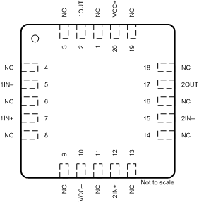
NC- no internal
connection
Figure 4-6 TL082 FK Package,20-Pin LCCC
(Top View)
Table 4-4 Pin Functions: TL082x
| PIN | TYPE(1) | DESCRIPTION | |
|---|---|---|---|
| NAME | NO. | ||
| 1IN– | 5 | I | Inverting input |
| 1IN+ | 7 | I | Noninverting input |
| 1OUT | 2 | O | Output |
| 2IN– | 15 | I | Inverting input |
| 2IN+ | 12 | I | Noninverting input |
| 2OUT | 17 | O | Output |
| NC | 1, 3, 4, 6, 8, 9, 11, 13, 14, 16, 18, 19 | — | Do not connect |
| VCC– | 10 | — | Power supply |
| VCC+ | 20 | — | Power supply |
(1) I = input, O = output
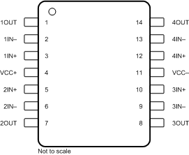 Figure 4-7 TL084x D, N, NS, PW, J, and DYY Package,
14-Pin SOIC, PDIP, SO, TSSOP, CDIP, and SOT-23 (14)
(Top View)
Table 4-5 Pin Functions: TL084x
| PIN | TYPE(1) | DESCRIPTION | |
|---|---|---|---|
| NAME | NO. | ||
| 1IN– | 2 | I | Inverting input |
| 1IN+ | 3 | I | Noninverting input |
| 1OUT | 1 | O | Output |
| 2IN– | 6 | I | Inverting input |
| 2IN+ | 5 | I | Noninverting input |
| 2OUT | 7 | O | Output |
| 3IN– | 9 | I | Inverting input |
| 3IN+ | 10 | I | Noninverting input |
| 3OUT | 8 | O | Output |
| 4IN– | 13 | I | Inverting input |
| 4IN+ | 12 | I | Noninverting input |
| 4OUT | 14 | O | Output |
| VCC– | 11 | — | Power supply |
| VCC+ | 4 | — | Power supply |
(1) I = input, O = output
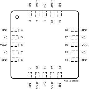
NC- no internal
connection
Figure 4-8 TL084 FK Package,20-Pin LCCC
(Top View)
Table 4-6 Pin Functions: TL084x
| PIN | TYPE(1) | DESCRIPTION | |
|---|---|---|---|
| NAME | NO. | ||
| 1IN– | 3 | I | Inverting input |
| 1IN+ | 4 | I | Noninverting input |
| 1OUT | 2 | O | Output |
| 2IN– | 9 | I | Inverting input |
| 2IN+ | 8 | I | Noninverting input |
| 2OUT | 10 | O | Output |
| 3IN– | 13 | I | Inverting input |
| 3IN+ | 14 | I | Noninverting input |
| 3OUT | 12 | O | Output |
| 4IN– | 19 | I | Inverting input |
| 4IN+ | 18 | I | Noninverting input |
| 4OUT | 20 | O | Output |
| NC | 1, 5, 7, 11, 15, 17 | — | Do not connect |
| VCC– | 16 | — | Power supply |
| VCC+ | 6 | — | Power supply |
(1) I = input, O = output