SLVS062N December 1991 – October 2016 TL1431 , TL1431M
PRODUCTION DATA.
- 1 Features
- 2 Applications
- 3 Description
- 4 Revision History
- 5 Pin Configuration and Functions
- 6 Specifications
- 7 Parameter Measurement Information
- 8 Detailed Description
- 9 Application and Implementation
- 10Power Supply Recommendations
- 11Layout
- 12Device and Documentation Support
- 13Mechanical, Packaging, and Orderable Information
Package Options
Mechanical Data (Package|Pins)
Thermal pad, mechanical data (Package|Pins)
Orderable Information
6 Specifications
6.1 Absolute Maximum Ratings
over operating free-air temperature range (unless otherwise noted)(1)| MIN | MAX | UNIT | ||
|---|---|---|---|---|
| Cathode voltage, VKA(2) | 37 | V | ||
| Continuous cathode current, IKA | –100 | 150 | mA | |
| Reference input current, II(ref) | –0.05 | 10 | mA | |
| Lead temperature, 1.6 mm (1/16 in) from case for 10 s | 260 | °C | ||
| Junction temperature, TJ | 150 | °C | ||
| Storage temperature, Tstg | –65 | 150 | °C | |
(1) Stresses beyond those listed under Absolute Maximum Ratings may cause permanent damage to the device. These are stress ratings only, and functional operation of the device at these or any other conditions beyond those indicated under recommended operating conditions is not implied. Exposure to absolute-maximum-rated conditions for extended periods may affect device reliability.
(2) All voltage values are with respect to ANODE, unless otherwise noted.
6.2 ESD Ratings – TL1431C, TL1431Q
| VALUE | UNIT | |||
|---|---|---|---|---|
| V(ESD) | Electrostatic discharge | Human-body model (HBM), per ANSI/ESDA/JEDEC JS-001(1) | ±2000 | V |
| Charged-device model (CDM), per JEDEC specification JESD22-C101(2) | ±1000 | |||
(1) JEDEC document JEP155 states that 500-V HBM allows safe manufacturing with a standard ESD control process.
(2) JEDEC document JEP157 states that 250-V CDM allows safe manufacturing with a standard ESD control process.
6.3 Recommended Operating Conditions
| MIN | MAX | UNIT | |||
|---|---|---|---|---|---|
| VKA | Cathode voltage | VI(ref) | 36 | V | |
| IKA | Cathode current | 1 | 100 | mA | |
| TA | Operating free-air temperature | TL1431C | 0 | 70 | °C |
| TL1431Q | –40 | 125 | |||
| TL1431M | –55 | 125 | |||
6.4 Thermal Information
| THERMAL METRIC(1) | TL1431 | TL1431M(2) | UNIT | ||||
|---|---|---|---|---|---|---|---|
| LP (TO-92) |
D (SOIC) |
PW (TSSOP) |
JG (CDIP) |
FK (LCCC) |
|||
| 3 PINS | 8 PINS | 8 PINS | 8 PINS | 20 PINS | |||
| RθJA | Junction-to-ambient thermal resistance | 157 | 114.7 | 172.4 | — | — | °C/W |
| RθJC(top) | Junction-to-case (top) thermal resistance | 80.7 | 59 | 55.2 | 69.7 | 55.5 | °C/W |
| RθJB | Junction-to-board thermal resistance | — | 55.4 | 100.8 | 99 | 54.2 | °C/W |
| ψJT | Junction-to-top characterization parameter | 24.6 | 12 | 5 | — | — | °C/W |
| ψJB | Junction-to-board characterization parameter | 136.4 | 54.8 | 99 | — | — | °C/W |
| RθJC(bot) | Junction-to-case (bottom) thermal resistance | — | — | — | 21 | 9.5 | °C/W |
(1) For more information about traditional and new thermal metrics, see the Semiconductor and IC Package Thermal Metrics application report.
(2) RθJC based on MIL-STD-883, and RθJB based on JESD51.
6.5 Electrical Characteristics – TL1431C
at specified free-air temperature and IKA = 10 mA (unless otherwise noted)| PARAMETER | TEST CONDITIONS | MIN | TYP | MAX | UNIT | ||
|---|---|---|---|---|---|---|---|
| VI(ref) | Reference input voltage | VKA = VI(ref)
(see Figure 13) |
TA = 25°C | 2490 | 2500 | 2510 | mV |
| TA = 0°C to 70°C | 2480 | 2520 | |||||
| VI(dev) | Deviation of reference input voltage over full temperature range(1) | VKA = VI(ref), TA = 0°C to 70°C (see Figure 13) |
4 | 20 | mV | ||
 |
Ratio of change in reference input voltage to the change in cathode voltage | ΔVKA = 3 V to 36 V, TA = 0°C to 70°C (see Figure 14) |
–1.1 | –2 | mV/V | ||
| II(ref) | Reference input current | R1 = 10 kΩ, R2 = ∞ (see Figure 14) |
TA = 25°C | 1.5 | 2.5 | µA | |
| TA = 0°C to 70°C | 3 | ||||||
| II(dev) | Deviation of reference input current over full temperature range(1) | R1 = 10 kΩ, R2 = ∞, TA = 0°C to 70°C (see Figure 14) |
0.2 | 1.2 | µA | ||
| Imin | Minimum cathode current for regulation | VKA = VI(ref), TA = 25°C (see Figure 13) | 0.45 | 1 | mA | ||
| Ioff | Off-state cathode current | VKA = 36 V, VI(ref) = 0 (see Figure 15) |
TA = 25°C | 0.18 | 0.5 | µA | |
| TA = 0°C to 70°C | 2 | ||||||
| |zKA| | Output impedance(2) | VKA = VI(ref), f ≤ 1 kHz, IKA = 1 mA to 100 mA, TA = 25°C (see Figure 13) |
0.2 | 0.4 | Ω | ||
(1) The deviation parameters VI(dev) and II(dev) are defined as the differences between the maximum and minimum values obtained over the rated temperature range. The average full-range temperature coefficient of the reference input voltage αVI(ref) is defined as:

αVI(ref) is positive or negative, depending on whether minimum VI(ref) or maximum VI(ref), respectively, occurs at the lower temperature.

αVI(ref) is positive or negative, depending on whether minimum VI(ref) or maximum VI(ref), respectively, occurs at the lower temperature.
(2) The output impedance is defined as: 
When the device is operating with two external resistors (see Figure 2), the total dynamic impedance of the circuit is given by: , which is approximately equal to
  .
.

When the device is operating with two external resistors (see Figure 2), the total dynamic impedance of the circuit is given by:
 , which is approximately equal to
  .
.6.6 Electrical Characteristics – TL1431Q
at specified free-air temperature and IKA = 10 mA (unless otherwise noted)| PARAMETER | TEST CONDITIONS | MIN | TYP | MAX | UNIT | ||
|---|---|---|---|---|---|---|---|
| VI(ref) | Reference input voltage | VKA = VI(ref)
(see Figure 13) |
TA = 25°C | 2490 | 2500 | 2510 | mV |
| TA = –40°C to 125°C | 2470 | 2530 | |||||
| VI(dev) | Deviation of reference input voltage over full temperature range(1) | VKA = VI(ref), TA = –40°C to 125°C (see Figure 13) |
17 | 55 | mV | ||
 |
Ratio of change in reference input voltage to the change in cathode voltage | ΔVKA = 3 V to 36 V, TA = –40°C to 125°C (see Figure 14) |
–1.1 | –2 | mV/V | ||
| II(ref) | Reference input current | R1 = 10 kΩ, R2 = ∞ (see Figure 14) |
TA = 25°C | 1.5 | 2.5 | µA | |
| TA = –40°C to 125°C | 4 | ||||||
| II(dev) | Deviation of reference input current over full temperature range(1) | R1 = 10 kΩ, R2 = ∞, TA = –40°C to 125°C (see Figure 14) |
0.5 | 2 | µA | ||
| Imin | Minimum cathode current for regulation | VKA = VI(ref), TA = 25°C (see Figure 13) | 0.45 | 1 | mA | ||
| Ioff | Off-state cathode current | VKA = 36 V, VI(ref) = 0 (see Figure 15) |
TA = 25°C | 0.18 | 0.5 | µA | |
| TA = –40°C to 125°C | 2 | ||||||
| |zKA| | Output impedance(2) | VKA = VI(ref), f ≤ 1 kHz, IKA = 1 mA to 100 mA, TA = 25°C (see Figure 13) |
0.2 | 0.4 | Ω | ||
(1) The deviation parameters VI(dev) and II(dev) are defined as the differences between the maximum and minimum values obtained over the rated temperature range. The average full-range temperature coefficient of the reference input voltage αVI(ref) is defined as:

αVI(ref) is positive or negative, depending on whether minimum VI(ref) or maximum VI(ref), respectively, occurs at the lower temperature.

αVI(ref) is positive or negative, depending on whether minimum VI(ref) or maximum VI(ref), respectively, occurs at the lower temperature.
(2) The output impedance is defined as: 
When the device is operating with two external resistors (see Figure 2), the total dynamic impedance of the circuit is given by: , which is approximately equal to
  .
.

When the device is operating with two external resistors (see Figure 2), the total dynamic impedance of the circuit is given by:
 , which is approximately equal to
  .
.6.7 Electrical Characteristics – TL1431M
at specified free-air temperature and IKA = 10 mA (unless otherwise noted)| PARAMETER | TEST CONDITIONS | MIN | TYP | MAX | UNIT | ||
|---|---|---|---|---|---|---|---|
| VI(ref) | Reference input voltage | VKA = VI(ref)
(see Figure 13) |
TA = 25°C | 2475 | 2500 | 2540 | mV |
| TA = –55°C to 125°C | 2460 | 2550 | |||||
| VI(dev) | Deviation of reference input voltage over full temperature range(1) | VKA = VI(ref), TA = –55°C to 125°C (see Figure 13) |
17 | 55(2) | mV | ||
 |
Ratio of change in reference input voltage to the change in cathode voltage | ΔVKA = 3 V to 36 V, TA = –55°C to 125°C (see Figure 14) |
–1.1 | –2 | mV/V | ||
| II(ref) | Reference input current | R1 = 10 kΩ, R2 = ∞ (see Figure 14) |
TA = 25°C | 1.5 | 2.5 | µA | |
| TA = –55°C to 125°C | 5 | ||||||
| II(dev) | Deviation of reference input current over full temperature range(1) | R1 = 10 kΩ, R2 = ∞, TA = –55°C to 125°C (see Figure 14) |
0.5 | 3(2) | µA | ||
| Imin | Minimum cathode current for regulation | VKA = VI(ref), TA = 25°C (see Figure 13) | 0.45 | 1 | mA | ||
| Ioff | Off-state cathode current | VKA = 36 V, VI(ref) = 0 (see Figure 15) |
TA = 25°C | 0.18 | 0.5 | µA | |
| TA = –55°C to 125°C | 2 | ||||||
| |zKA| | Output impedance(3) | VKA = VI(ref), f ≤ 1 kHz, IKA = 1 mA to 100 mA, TA = 25°C (see Figure 13) |
0.2 | 0.4 | Ω | ||
(1) The deviation parameters VI(dev) and II(dev) are defined as the differences between the maximum and minimum values obtained over the rated temperature range. The average full-range temperature coefficient of the reference input voltage αVI(ref) is defined as:

αVI(ref) is positive or negative, depending on whether minimum VI(ref) or maximum VI(ref), respectively, occurs at the lower temperature.

αVI(ref) is positive or negative, depending on whether minimum VI(ref) or maximum VI(ref), respectively, occurs at the lower temperature.
(2) On products compliant to MIL-PRF-38535, this parameter is not production tested.
(3) The output impedance is defined as: 
When the device is operating with two external resistors (see Figure 2), the total dynamic impedance of the circuit is given by: , which is approximately equal to
  .
.

When the device is operating with two external resistors (see Figure 2), the total dynamic impedance of the circuit is given by:
 , which is approximately equal to
  .
.6.8 Typical Characteristics
Data at high and low temperatures are applicable only within the recommended operating free-air temperature ranges of the various devices.Table 1. Table Of Graphs
| GRAPH | FIGURE |
|---|---|
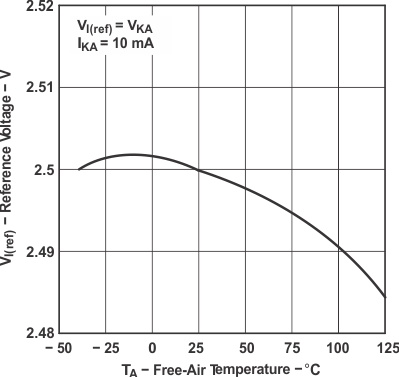
| Reference voltage vs Free-air temperature | Figure 1 |
| Reference current vs Fire-air temperature | Figure 2 |
| Cathode current vs Cathode voltage | Figure 3, Figure 4 |
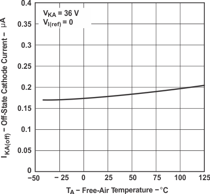
| Off-state cathode current vs Free-air temperature | Figure 5 |
| Ratio of delta reference voltage to delta cathode voltage vs Free-air temperature | Figure 6 |
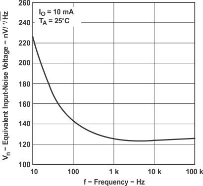
| Equivalent input-noise voltage vs Frequency | Figure 7 |
| Equivalent input-noise voltage over a 10-second period | Figure 8 |
| Small-signal voltage amplification vs Frequency | Figure 9 |
| Reference impedance vs Frequency | Figure 10 |
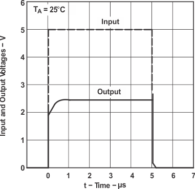
| Pulse response | Figure 11 |
| Stability boundary conditions | Figure 12 |
 Figure 1. Reference Voltage vs Free-Air Temperature
 Figure 3. Cathode Current vs Cathode Voltage
 Figure 5. Off-State Cathode Current vs Free-Air Temperature
 Figure 7. Equivalent Input-Noise Voltage vs Frequency
 Figure 9. Small-Signal Voltage Amplification vs Frequency

 Figure 2. Reference Current vs Free-Air Temperature
 Figure 4. Cathode Current vs Cathode Voltage
 Figure 6. Ratio Of Delta Reference Voltage
To Delta Cathode Voltage vs Free-Air Temperature
 Figure 8. Equivalent Input-Noise Voltage
Over A 10-S Period
 Figure 10. Reference Impedance vs Frequency

The areas under the curves represent conditions that may cause the device to oscillate. For curves B, C, and D, R2 and V+ are adjusted to establish the initial VKA and IKA conditions, with CL = 0. VBATT and CL then are adjusted to determine the ranges of stability.
Figure 12. Stability Boundary Conditions