SLLSF10 December 2019 TL16C750E
PRODUCTION DATA.
- 1 Features
- 2 Applications
- 3 Description
- 4 Revision History
- 5 Description (continued)
- 6 Pin Configuration and Functions
- 7 Specifications
- 8 Parameter Measurement Information
-
9 Detailed Description
- 9.1 Overview
- 9.2 Functional Block Diagrams
- 9.3
Feature Description
- 9.3.1 UART Modes
- 9.3.2 Trigger Levels
- 9.3.3 Hardware Flow Control
- 9.3.4 Auto-RTS
- 9.3.5 Auto-CTS
- 9.3.6 Software Flow Control
- 9.3.7 Software Flow Control Example
- 9.3.8 Reset
- 9.3.9 Interrupts
- 9.3.10 Interrupt Mode Operation
- 9.3.11 Polled Mode Operation
- 9.3.12 Break and Timeout Conditions
- 9.3.13 Programmable Baud Rate Generator with Fractional Divisor
- 9.3.14 Fractional Divisor
- 9.4 Device Functional Modes
- 9.5
Register Maps
- 9.5.1 Registers Operations
- 9.5.2 Receiver Holding Register (RHR)
- 9.5.3 Transmit Holding Register (THR)
- 9.5.4 FIFO Control Register (FCR)
- 9.5.5 Line Control Register (LCR)
- 9.5.6 Line Status Register (LSR)
- 9.5.7 Modem Control Register (MCR)
- 9.5.8 Modem Status Register (MSR)
- 9.5.9 Interrupt Enable Register (IER)
- 9.5.10 Interrupt Identification Register (IIR)
- 9.5.11 Enhanced Feature Register (EFR)
- 9.5.12 Divisor Latches (DLL, DLH, DLF)
- 9.5.13 Transmission Control Register (TCR)
- 9.5.14 Trigger Level Register (TLR)
- 9.5.15 FIFO Ready Register
- 9.5.16 Alternate Function Register (AFR)
- 9.5.17 RS-485 Mode
- 9.5.18 IrDA Overview
- 9.5.19 IrDA Encoder Function
- 10Application and Implementation
- 11Power Supply Recommendations
- 12Layout
- 13Device and Documentation Support
- 14Mechanical, Packaging, and Orderable Information
Package Options
Mechanical Data (Package|Pins)
- PFB|48
Thermal pad, mechanical data (Package|Pins)
Orderable Information
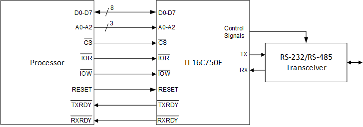
10.2 Typical Application
The typical application is to communicate over UART, either through a RS-232 transceiver, or directly. The general initialization sequence is recommended as following:
- Set the desired baud rate with DLL and DLH (or with fractional baud rate if required)
- Set the desired word length and other settings in the LCR register.
- Reset the FIFOs with the FCR registers
 Figure 43. Typical Application