SLLS646C March 2008 – June 2017 TL16C752C
PRODUCTION DATA.
- 1 Features
- 2 Applications
- 3 Description
- 4 Revision History
- 5 Description (continued)
- 6 Pin Configuration and Functions
- 7 Specifications
-
8 Detailed Description
- 8.1 Overview
- 8.2 Functional Block Diagram
- 8.3
Feature Description
- 8.3.1
Functional Description
- 8.3.1.1 Trigger Levels
- 8.3.1.2 Hardware Flow Control
- 8.3.1.3 Auto-RTS
- 8.3.1.4 Auto-CTS
- 8.3.1.5 Software Flow Control
- 8.3.1.6 Software Flow Control Example
- 8.3.1.7 Reset
- 8.3.1.8 Interrupts
- 8.3.1.9 Interrupt Mode Operation
- 8.3.1.10 Polled Mode Operation
- 8.3.1.11 Break and Timeout Conditions
- 8.3.1.12 Programmable Baud Rate Generator
- 8.3.1
Functional Description
- 8.4 Device Functional Modes
- 8.5
Register Maps
- 8.5.1 Principals of Operation
- 8.5.2 Receiver Holding Register (RHR)
- 8.5.3 Transmit Holding Register (THR)
- 8.5.4 FIFO Control Register (FCR)
- 8.5.5 Line Control Register (LCR)
- 8.5.6 Line Status Register (LSR)
- 8.5.7 Modem Control Register (MCR)
- 8.5.8 Modem Status Register (MSR)
- 8.5.9 Interrupt Enable Register (IER)
- 8.5.10 Interrupt Identification Register (IIR)
- 8.5.11 Enhanced Feature Register (EFR)
- 8.5.12 Divisor Latches (DLL, DLH)
- 8.5.13 Transmission Control Register (TCR)
- 8.5.14 Trigger Level Register (TLR)
- 8.5.15 FIFO Ready Register
- 8.5.16 Alternate Function Register (AFR)
- 8.5.17 RS-485 Mode
- 8.5.18 IrDA Overview
- 8.5.19 IrDA Encoder Function
- 9 Application and Implementation
- 10Power Supply Recommendations
- 11Layout
- 12Device and Documentation Support
- 13Mechanical, Packaging, and Orderable Information
Package Options
Mechanical Data (Package|Pins)
Thermal pad, mechanical data (Package|Pins)
- RHB|32
Orderable Information
7 Specifications
7.1 Absolute Maximum Ratings
over operating free-air temperature range (unless otherwise noted)(1)| MIN | MAX | UNIT | |||
|---|---|---|---|---|---|
| VCC | Supply voltage | –0.5 | 6 | V | |
| VI | Input voltage | –0.5 | VCC + 0.5 | V | |
| VO | Output voltage | –0.5 | VCC + 0.5 | V | |
| TA | Operating free-air temperature | TL16C752C | 0 | 70 | °C |
| TL16C752CI | –40 | 85 | |||
| Tstg | Storage temperature | –65 | 150 | °C | |
(1) Stresses beyond those listed under Absolute Maximum Ratings may cause permanent damage to the device. These are stress ratings only and functional operation of the device at these or any other conditions beyond those indicated under Recommended Operating Conditions is not implied. Exposure to absolute-maximum-rated conditions for extended periods may affect device reliability.
7.2 ESD Ratings
| VALUE | UNIT | |||
|---|---|---|---|---|
| V(ESD) | Electrostatic discharge | Human-body model (HBM), per ANSI/ESDA/JEDEC JS-001(1) | ±2000 | V |
| Charged-device model (CDM), per JEDEC specification JESD22-C101(2) | ±500 | |||
(1) JEDEC document JEP155 states that 500-V HBM allows safe manufacturing with a standard ESD control process.
(2) JEDEC document JEP157 states that 250-V CDM allows safe manufacturing with a standard ESD control process.
7.3 Recommended Operating Conditions
over operating free-air temperature range (unless otherwise noted)7.4 Thermal Information
| THERMAL METRIC(1) | TL16C752C | UNIT | |
|---|---|---|---|
| PFB (TQFP) | |||
| 48 PINS | |||
| RθJA | Junction-to-ambient thermal resistance | 61 | °C/W |
| RθJC(top) | Junction-to-case (top) thermal resistance | 17.3 | °C/W |
| RθJC(bot) | Junction-to-case (bottom) thermal resistance | N/A | °C/W |
(1) For more information about traditional and new thermal metrics, see the Semiconductor and IC Package Thermal Metrics application report.
7.5 Electrical Characteristics
over operating free-air temperature range (unless otherwise noted)7.6 Timing Requirements
TA = 0°C to 70°C, VCC = 1.8 V to 5 V ±10% (unless otherwise noted)| LIMITS | UNIT | ||||||||||
|---|---|---|---|---|---|---|---|---|---|---|---|
| 1.8 V | 2.5 V | 3.3 V | 5 V | ||||||||
| MIN | MAX | MIN | MAX | MIN | MAX | MIN | MAX | ||||
| tRESET | Reset pulse width | 200 | 200 | 200 | 200 | ns | |||||
| CP | CP clock period | 63 | 42 | 32 | 20 | ns | |||||
| t3w | Oscillator or clock speed | 16 | 24 | 32 | 48 | MHz | |||||
| t6s | Address setup time | 20 | 15 | 10 | 5 | ns | |||||
| t6h | Address hold time | See Figure 1 and Figure 2 | 15 | 10 | 7 | 5 | ns | ||||
| t7w | IOR strobe width | See Figure 1 and Figure 2 | 85 | 70 | 50 | 40 | ns | ||||
| t9d | Read cycle delay | See Figure 2 | 85 | 70 | 60 | 50 | ns | ||||
| t12d | Delay from IOR to data | See Figure 2 | 65 | 50 | 35 | 25 | ns | ||||
| t12h | Data disable time | 35 | 25 | 20 | 15 | ns | |||||
| t13w | IOW strobe width | See Figure 1 | 85 | 70 | 50 | 40 | ns | ||||
| t15d | Write cycle delay | See Figure 1 | 85 | 70 | 60 | 50 | ns | ||||
| t16s | Data setup time | See Figure 1 | 40 | 30 | 20 | 15 | ns | ||||
| t16h | Data hold time | See Figure 1 | 35 | 25 | 15 | 10 | ns | ||||
| t17d | Delay from IOW to output | 50-pF load, see Figure 3 | 60 | 40 | 30 | 20 | ns | ||||
| t18d | Delay to set interrupt from MODEM input | 50-pF load, see Figure 3 | 70 | 55 | 45 | 35 | ns | ||||
| t19d | Delay to reset interrupt from IOR | 50-pF load | 80 | 55 | 40 | 30 | ns | ||||
| t20d | Delay from stop to set interrupt | See Figure 4 | 1 | 1 | 1 | 1 | baudrate | ||||
| t21d | Delay from IOR to reset interrupt | 50-pF load, see Figure 4 | 55 | 45 | 35 | 25 | ns | ||||
| t22d | Delay from stop to interrupt | See Figure 7 | 1 | 1 | 1 | 1 | baudrate | ||||
| t23d | Delay from initial IOW reset to transmit start | See Figure 7 | 8 | 24 | 8 | 24 | 8 | 24 | 8 | 24 | baudrate |
| t24d | Delay from IOW to reset interrupt | See Figure 7 | 75 | 45 | 35 | 25 | ns | ||||
| t25d | Delay from stop to set RXRDY | See Figure 5 and Figure 6 | 1 | 1 | 1 | 1 | baudrate | ||||
| t26d | Delay from IOR to reset RXRDY | See Figure 5 and Figure 6 | 1 | 1 | 1 | 1 | μs | ||||
| t27d | Delay from IOW to set TXRDY | See Figure 8 and Figure 9 | 70 | 60 | 50 | 40 | ns | ||||
| t28d | Delay from start to reset TXRDY | See Figure 8 and Figure 9 | 16 | 16 | 16 | 16 | baudrate | ||||
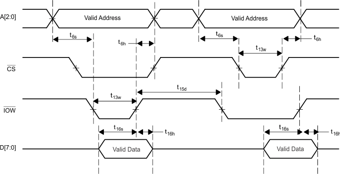 Figure 1. General Write Timing
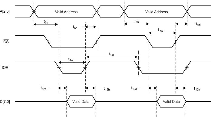 Figure 2. General Read Timing
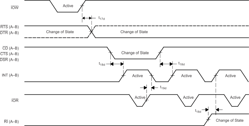 Figure 3. Modem or Output Timing
 Figure 4. Receive Timing
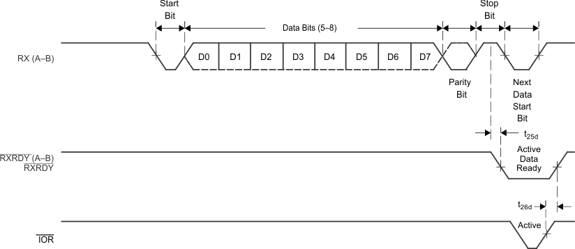 Figure 5. Receive Ready Timing in Non-FIFO Mode
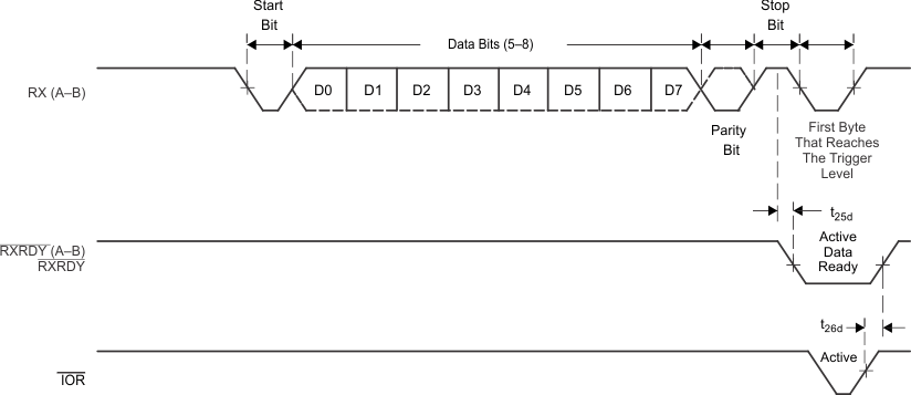 Figure 6. Receive Timing in FIFO Mode
 Figure 7. Transmit Timing
 Figure 8. Transmit Ready Timing in Non-FIFO Mode
 Figure 9. Transmit Timing in FIFO Mode
7.7 Typical Characteristics
all channels active, TA = 25°C, unless otherwise noted
(VCC = 1.62, 1.8, and 1.98 V)

(VCC = 3, 3.3, and 3.5 V)

(VCC = 2.25, 2.5, and 2.75 V)
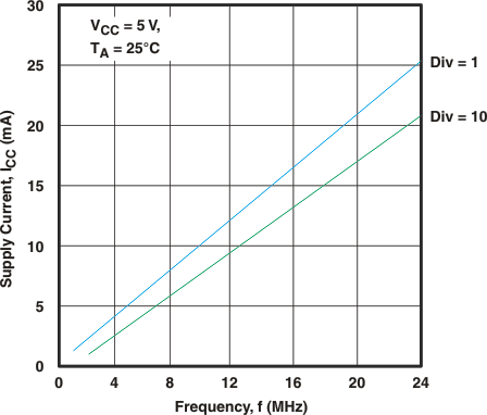 Figure 13. Supply Current vs Frequency
(VCC = 5 V)