SLVS038J January   1989  – October 2024 TL2842 , TL2843 , TL2844 , TL2845 , TL3842 , TL3843 , TL3844 , TL3845

PRODUCTION DATA  

  1.   1
  2. Features
  3. Applications
  4. Description
  5. Pin Configuration and Functions
  6. Specifications
    1. 5.1 Absolute Maximum Ratings
    2. 5.2 ESD Ratings
    3. 5.3 Recommended Operating Conditions
    4. 5.4 Thermal Information
    5. 5.5 Electrical Characteristics
    6. 5.6 Typical Characteristics
  7. Detailed Description
    1. 6.1 Overview
    2. 6.2 Functional Block Diagram
    3. 6.3 Feature Description
      1. 6.3.1 Pulse-by-Pulse Current Limiting
      2. 6.3.2 Error Amplifier With Low Output Resistance
      3. 6.3.3 High-Current Totem-Pole Output
    4. 6.4 Device Functional Modes
      1. 6.4.1 Shutdown Technique
      2. 6.4.2 Slope Compensation
  8. Application and Implementation
    1. 7.1 Typical Application
      1. 7.1.1 Design Requirements
      2. 7.1.2 Detailed Design Procedure
        1. 7.1.2.1 Current-Sense Circuit
        2. 7.1.2.2 Error-Amplifier Configuration
        3. 7.1.2.3 Oscillator Section
      3. 7.1.3 Application Curve
    2. 7.2 Power Supply Recommendations
    3. 7.3 Layout
      1. 7.3.1 Layout Guidelines
        1. 7.3.1.1 Feedback Traces
        2. 7.3.1.2 Input/Output Capacitors
        3. 7.3.1.3 Compensation Components
        4. 7.3.1.4 Traces and Ground Planes
      2. 7.3.2 Layout Example
  9. Device and Documentation Support
    1. 8.1 Receiving Notification of Documentation Updates
    2. 8.2 Support Resources
    3. 8.3 Trademarks
    4. 8.4 Electrostatic Discharge Caution
    5. 8.5 Glossary
  10. Revision History
  11. 10Mechanical, Packaging, and Orderable Information

Package Options

Refer to the PDF data sheet for device specific package drawings

Mechanical Data (Package|Pins)
  • D|14
  • D|8
  • P|8
Thermal pad, mechanical data (Package|Pins)
Orderable Information

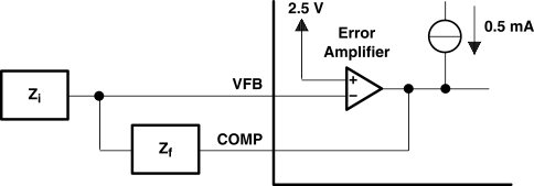
Error-Amplifier Configuration

TL2842 TL2843 TL2844 TL2845   TL3842 TL3843 TL3844 TL3845 Error-Amplifier Configuration Schematic
Error amplifier can source or sink up to 0.5 mA.
Figure 7-3 Error-Amplifier Configuration Schematic