SLVS038J January   1989  – October 2024 TL2842 , TL2843 , TL2844 , TL2845 , TL3842 , TL3843 , TL3844 , TL3845

PRODUCTION DATA  

  1.   1
  2. Features
  3. Applications
  4. Description
  5. Pin Configuration and Functions
  6. Specifications
    1. 5.1 Absolute Maximum Ratings
    2. 5.2 ESD Ratings
    3. 5.3 Recommended Operating Conditions
    4. 5.4 Thermal Information
    5. 5.5 Electrical Characteristics
    6. 5.6 Typical Characteristics
  7. Detailed Description
    1. 6.1 Overview
    2. 6.2 Functional Block Diagram
    3. 6.3 Feature Description
      1. 6.3.1 Pulse-by-Pulse Current Limiting
      2. 6.3.2 Error Amplifier With Low Output Resistance
      3. 6.3.3 High-Current Totem-Pole Output
    4. 6.4 Device Functional Modes
      1. 6.4.1 Shutdown Technique
      2. 6.4.2 Slope Compensation
  8. Application and Implementation
    1. 7.1 Typical Application
      1. 7.1.1 Design Requirements
      2. 7.1.2 Detailed Design Procedure
        1. 7.1.2.1 Current-Sense Circuit
        2. 7.1.2.2 Error-Amplifier Configuration
        3. 7.1.2.3 Oscillator Section
      3. 7.1.3 Application Curve
    2. 7.2 Power Supply Recommendations
    3. 7.3 Layout
      1. 7.3.1 Layout Guidelines
        1. 7.3.1.1 Feedback Traces
        2. 7.3.1.2 Input/Output Capacitors
        3. 7.3.1.3 Compensation Components
        4. 7.3.1.4 Traces and Ground Planes
      2. 7.3.2 Layout Example
  9. Device and Documentation Support
    1. 8.1 Receiving Notification of Documentation Updates
    2. 8.2 Support Resources
    3. 8.3 Trademarks
    4. 8.4 Electrostatic Discharge Caution
    5. 8.5 Glossary
  10. Revision History
  11. 10Mechanical, Packaging, and Orderable Information

Package Options

Refer to the PDF data sheet for device specific package drawings

Mechanical Data (Package|Pins)
  • D|8
  • D|14
  • P|8
Thermal pad, mechanical data (Package|Pins)
Orderable Information

Shutdown Technique

The PWM controller (see Figure 6-1) can be shut down by two methods: either raise the voltage at ISENSE above 1 V or pull the COMP terminal below a voltage two diode drops above ground. Either method causes the output of the PWM comparator to be high (see Functional Block Diagram). The PWM latch is reset dominant so that the output remains low until the next clock cycle after the shutdown condition at the COMP or ISENSE terminal is removed. In one example, an externally latched shutdown can be accomplished by adding an SCR that resets by cycling VCC below the lower UVLO threshold. At this point, the reference turns off, allowing the SCR to reset.
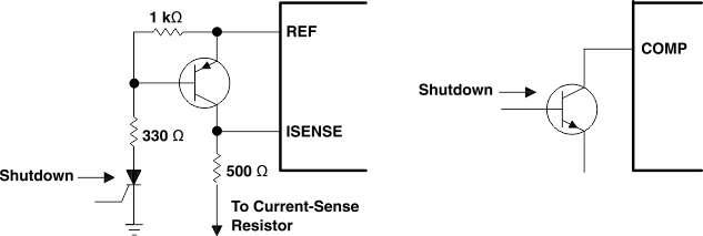
TL2842 TL2843 TL2844 TL2845   TL3842 TL3843 TL3844 TL3845 Shutdown TechniquesFigure 6-1 Shutdown Techniques