SLVS038J January 1989 – October 2024 TL2842 , TL2843 , TL2844 , TL2845 , TL3842 , TL3843 , TL3844 , TL3845
PRODUCTION DATA
- 1
- 1 Features
- 2 Applications
- 3 Description
- 4 Pin Configuration and Functions
- 5 Specifications
- 6 Detailed Description
- 7 Application and Implementation
- 8 Device and Documentation Support
- 9 Revision History
- 10Mechanical, Packaging, and Orderable Information
Package Options
Refer to the PDF data sheet for device specific package drawings
Mechanical Data (Package|Pins)
- D|14
- D|8
- P|8
Thermal pad, mechanical data (Package|Pins)
Orderable Information
3 Description
The TL284x and TL384x series of control integrated circuits provide the features that are necessary to implement off-line or DC-to-DC fixed-frequency current-mode control schemes, with a minimum number of external components. Some of the internally implemented circuits are an undervoltage lockout (UVLO), featuring a start-up current of less than 1mA, and a precision reference trimmed for accuracy at the error amplifier input. Other internal circuits include logic to ensure latched operation, a pulse-width modulation (PWM) comparator (that also provides current-limit control), and a totem-pole output stage designed to source or sink high-peak current. The output stage, suitable for driving N-channel MOSFETs, is low when it is in the off state.
| PART NUMBER | PACKAGE(1) | PACKAGE SIZE(2) |
|---|---|---|
| TLx84x | D (SOIC, 8) | 4.90mm × 6.00mm |
| D (SOIC, 14) | 8.65mm × 6.00mm | |
| P (PDIP, 8) | 9.81mm × 9.43mm |
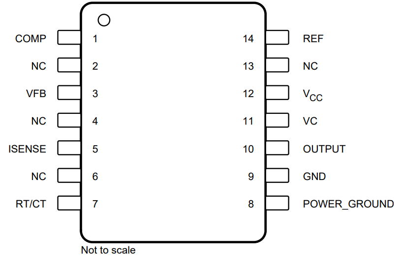
 D Package14-Pin SOICTop View
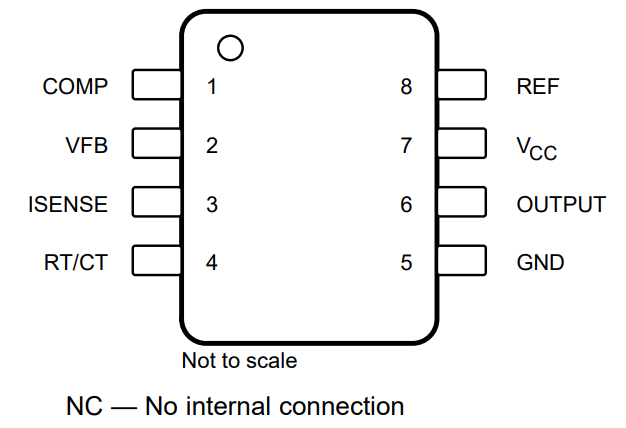
 D or P
Package8-Pin SOIC or PDIPTop View