SLVS038J January   1989  – October 2024 TL2842 , TL2843 , TL2844 , TL2845 , TL3842 , TL3843 , TL3844 , TL3845

PRODUCTION DATA  

  1.   1
  2. Features
  3. Applications
  4. Description
  5. Pin Configuration and Functions
  6. Specifications
    1. 5.1 Absolute Maximum Ratings
    2. 5.2 ESD Ratings
    3. 5.3 Recommended Operating Conditions
    4. 5.4 Thermal Information
    5. 5.5 Electrical Characteristics
    6. 5.6 Typical Characteristics
  7. Detailed Description
    1. 6.1 Overview
    2. 6.2 Functional Block Diagram
    3. 6.3 Feature Description
      1. 6.3.1 Pulse-by-Pulse Current Limiting
      2. 6.3.2 Error Amplifier With Low Output Resistance
      3. 6.3.3 High-Current Totem-Pole Output
    4. 6.4 Device Functional Modes
      1. 6.4.1 Shutdown Technique
      2. 6.4.2 Slope Compensation
  8. Application and Implementation
    1. 7.1 Typical Application
      1. 7.1.1 Design Requirements
      2. 7.1.2 Detailed Design Procedure
        1. 7.1.2.1 Current-Sense Circuit
        2. 7.1.2.2 Error-Amplifier Configuration
        3. 7.1.2.3 Oscillator Section
      3. 7.1.3 Application Curve
    2. 7.2 Power Supply Recommendations
    3. 7.3 Layout
      1. 7.3.1 Layout Guidelines
        1. 7.3.1.1 Feedback Traces
        2. 7.3.1.2 Input/Output Capacitors
        3. 7.3.1.3 Compensation Components
        4. 7.3.1.4 Traces and Ground Planes
      2. 7.3.2 Layout Example
  9. Device and Documentation Support
    1. 8.1 Receiving Notification of Documentation Updates
    2. 8.2 Support Resources
    3. 8.3 Trademarks
    4. 8.4 Electrostatic Discharge Caution
    5. 8.5 Glossary
  10. Revision History
  11. 10Mechanical, Packaging, and Orderable Information

Package Options

Refer to the PDF data sheet for device specific package drawings

Mechanical Data (Package|Pins)
  • D|8
  • D|14
  • P|8
Thermal pad, mechanical data (Package|Pins)
Orderable Information

Typical Application

The following application is an open-loop laboratory test fixture. This circuit demonstrates the setup and use of the TL284x and TL384x devices and their internal circuitry.

In the open-loop laboratory test fixture (see Figure 7-1), high peak currents associated with loads necessitate careful grounding techniques. Timing and bypass capacitors should be connected close to the GND terminal in a single-point ground. The transistor and 5-kΩ potentiometer sample the oscillator waveform and apply an adjustable ramp to the ISENSE terminal.
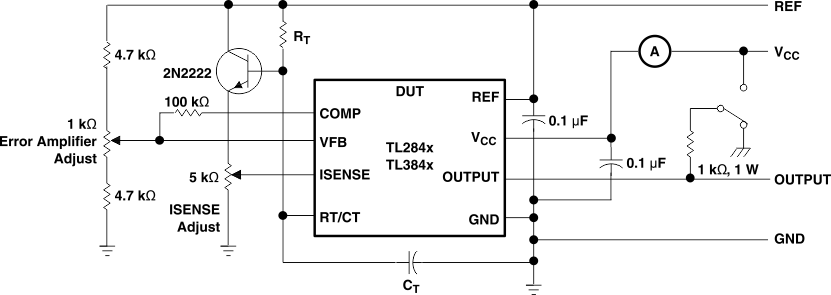
TL2842 TL2843 TL2844 TL2845   TL3842 TL3843 TL3844 TL3845 Open-Loop Laboratory Test FixtureFigure 7-1 Open-Loop Laboratory Test Fixture