SLVS610C August 2006 – October 2024
PRODUCTION DATA
- 1
- 1 Features
- 2 Applications
- 3 Description
- 4 Pin Configuration and Functions
-
5 Specifications
- 5.1 Absolute Maximum Ratings
- 5.2 ESD Ratings
- 5.3 Recommended Operating Conditions
- 5.4 Thermal Information
- 5.5 Reference Section Electrical Characteristics
- 5.6 Oscillator Section Electrical Characteristics
- 5.7 Error-Amplifier Section Electrical Characteristics
- 5.8 Current-Sense Section Electrical Characteristics
- 5.9 Output Section Electrical Characteristics
- 5.10 Undervoltage-Lockout Section Electrical Characteristics
- 5.11 Pulse-Width Modulator Section Electrical Characteristics
- 5.12 Supply Voltage Electrical Characteristics
- 5.13 Typical Characteristics
- 6 Detailed Description
- 7 Application and Implementation
- 8 Device and Documentation Support
- 9 Revision History
- 10Mechanical, Packaging, and Orderable Information
Package Options
Mechanical Data (Package|Pins)
Thermal pad, mechanical data (Package|Pins)
Orderable Information
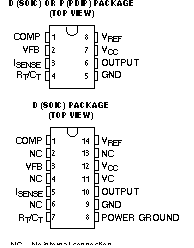
4 Pin Configuration and Functions

| PIN | Type(1) | DESCRIPTION | ||
|---|---|---|---|---|
| NAME | D (14 pins) | D or P (8 pins) | ||
| COMP | 1 | 1 | I/O | Error amplifier compensation pin |
| GND | 9 | 5 | - | Device power supply ground terminal |
| ISENSE | 5 | 3 | I | Current sense comparator input |
| NC | 2, 4, 6, 13 | - | - | Do not connect |
| OUTPUT | 10 | 6 | O | PWM Output |
| POWER GROUND | 8 | - | - | Output PWM ground terminal |
| REF | 14 | 8 | O | Oscillator voltage reference |
| RT/CT | 7 | 4 | I/O | Oscillator RC input |
| VC | 11 | - | - | Output PWM positive voltage supply |
| VCC | 12 | 7 | - | Device positive voltage supply |
| VFB | 3 | 2 | I | Error amplifier input |
(1) I = Input; O = Output; I/O = Input or Output