SLVS543S August 2004 – May 2024 TL431 , TL432
PRODUCTION DATA
- 1
- 1 Features
- 2 Applications
- 3 Description
- 4 Device Comparison Table
- 5 Pin Configuration and Functions
-
6 Specifications
- 6.1 Absolute Maximum Ratings
- 6.2 ESD Ratings
- 6.3 Thermal Information
- 6.4 Recommended Operating Conditions
- 6.5 Electrical Characteristics, TL431C, TL432C
- 6.6 Electrical Characteristics, TL431I, TL432I
- 6.7 Electrical Characteristics, TL431Q, TL432Q
- 6.8 Electrical Characteristics, TL431AC, TL432AC
- 6.9 Electrical Characteristics, TL431AI, TL432AI
- 6.10 Electrical Characteristics, TL431AQ, TL432AQ
- 6.11 Electrical Characteristics, TL431BC, TL432BC
- 6.12 Electrical Characteristics, TL431BI, TL432BI
- 6.13 Electrical Characteristics, TL431BQ, TL432BQ
- 6.14 Typical Characteristics
- 7 Parameter Measurement Information
- 8 Detailed Description
- 9 Applications and Implementation
- 10Device and Documentation Support
- 11Revision History
- 12Mechanical, Packaging, and Orderable Information
Package Options
Mechanical Data (Package|Pins)
Thermal pad, mechanical data (Package|Pins)
- PK|3
Orderable Information
6.14 Typical Characteristics
Data at high and low temperatures are applicable only within the recommended operating free-air temperature ranges of the various devices.
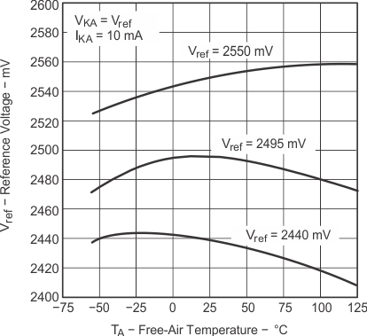 Figure 6-1 Reference Voltage vs Free-Air Temperature
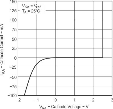 Figure 6-3 Cathode Current vs Cathode Voltage
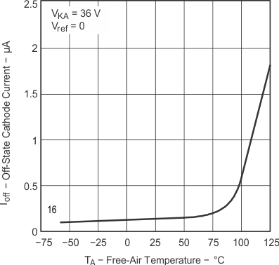 Figure 6-5 Off-State Cathode Current vs Free-Air Temperature
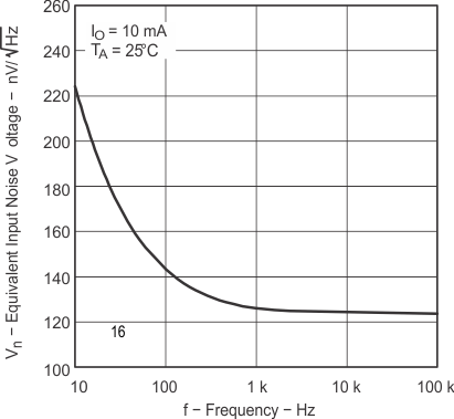 Figure 6-7 Equivalent Input Noise Voltage vs Frequency
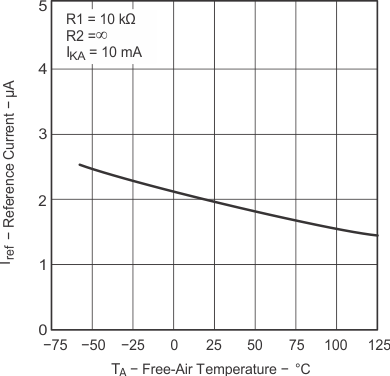 Figure 6-2 Reference Current vs Free-Air Temperature
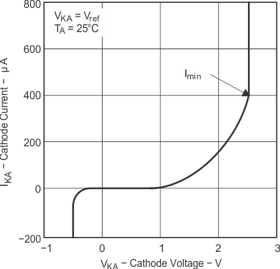 Figure 6-4 Cathode Current vs Cathode Voltage
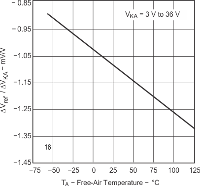 Figure 6-6 Ratio of Delta Reference Voltage to Delta Cathode Voltage vs Free-Air Temperature
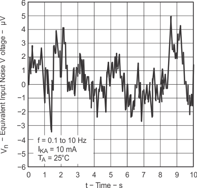 Figure 6-8 Equivalent Input Noise Voltage Over
a 10S Period
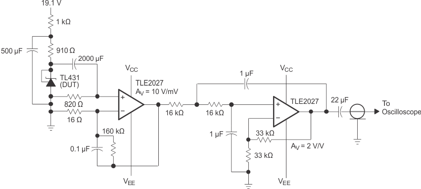 Figure 6-9 Test Circuit for Equivalent Input Noise
Voltage Over a 10S Period
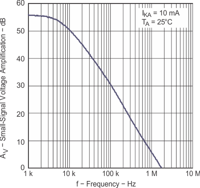 Figure 6-10 Small-Signal Voltage Amplification
vs Frequency
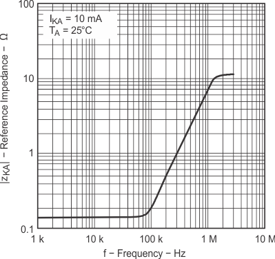 Figure 6-12 Reference
Impedance vs Frequency
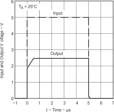 Figure 6-14 Pulse
Response
|
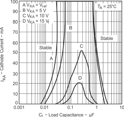
The areas under the curves represent conditions that can cause the device to oscillate. For curves B, C, and D, R2 and V+ are adjusted to establish the initial VKA and IKA conditions, with CL = 0. VBATT and CL then are adjusted to determine the ranges of stability. |
|
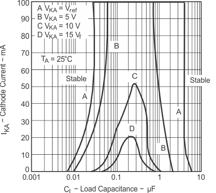
The areas under the curves represent conditions that can cause the device to oscillate. For curves B, C, and D, R2 and V+ are adjusted to establish the initial VKA and IKA conditions, with CL = 0. VBATT and CL then are adjusted to determine the ranges of stability. |
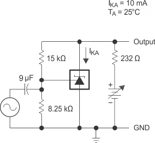 Figure 6-11 Test Circuit
for Voltage Amplification
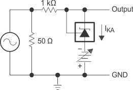 Figure 6-13 Test Circuit
for Reference Impedance
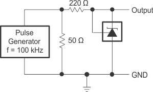 Figure 6-15 Test Circuit
for Pulse Response
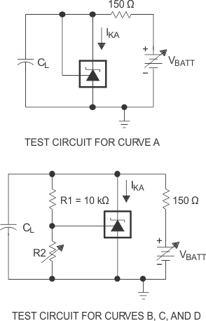 Figure 6-17 Test Circuits
for Stability Boundary Conditions
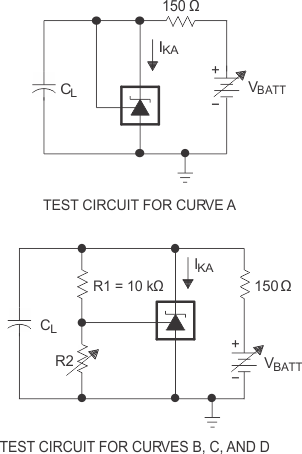 Figure 6-19 Test
Circuit for Stability Boundary Conditions