SGLS380I September   2008  – May 2024 TL720M05-Q1

PRODMIX  

  1.   1
  2. Features
  3. Applications
  4. Description
  5. Pin Configuration and Functions
  6. Specifications
    1. 5.1 Absolute Maximum Ratings
    2. 5.2 ESD Ratings
    3. 5.3 Recommended Operating Conditions
    4. 5.4 Thermal Information
    5. 5.5 Electrical Characteristics
    6. 5.6 Typical Characteristics
  7. Parameter Measurement Information
  8. Detailed Description
    1. 7.1 Overview
    2. 7.2 Functional Block Diagrams
    3. 7.3 Feature Description
      1. 7.3.1 Undervoltage Lockout
      2. 7.3.2 Thermal Shutdown
      3. 7.3.3 Current Limit
    4. 7.4 Device Functional Modes
      1. 7.4.1 Normal Operation
      2. 7.4.2 Dropout Operation
      3. 7.4.3 Disabled
  9. Application and Implementation
    1. 8.1 Application Information
      1. 8.1.1 Input and Output Capacitor Selection
        1. 8.1.1.1 Legacy Chip Capacitor Selection
        2. 8.1.1.2 New Chip Output Capacitor
        3. 8.1.1.3 New Chip Input Capacitor
      2. 8.1.2 Dropout Voltage
      3. 8.1.3 Reverse Current
      4. 8.1.4 Power Dissipation (PD)
        1. 8.1.4.1 Thermal Performance Versus Copper Area
        2. 8.1.4.2 Power Dissipation Versus Ambient Temperature
      5. 8.1.5 Estimating Junction Temperature
    2. 8.2 Typical Application
      1. 8.2.1 Design Requirements
      2. 8.2.2 Detailed Design Procedure
        1. 8.2.2.1 Input Capacitor
        2. 8.2.2.2 Output Capacitor
      3. 8.2.3 Application Curves
    3. 8.3 Power Supply Recommendations
    4. 8.4 Layout
      1. 8.4.1 Layout Guidelines
      2. 8.4.2 Layout Examples
  10. Device and Documentation Support
    1. 9.1 Device Support
      1. 9.1.1 Evaluation Module
      2. 9.1.2 Device Nomenclature
      3. 9.1.3 Development Support
    2. 9.2 Documentation Support
      1. 9.2.1 Related Documentation
    3. 9.3 Receiving Notification of Documentation Updates
    4. 9.4 Support Resources
    5. 9.5 Trademarks
    6. 9.6 Electrostatic Discharge Caution
    7. 9.7 Glossary
  11. 10Revision History
  12. 11Mechanical, Packaging, and Orderable Information

Package Options

Refer to the PDF data sheet for device specific package drawings

Mechanical Data (Package|Pins)
  • KVU|3
  • PWP|20
  • KTT|3
Thermal pad, mechanical data (Package|Pins)
Orderable Information

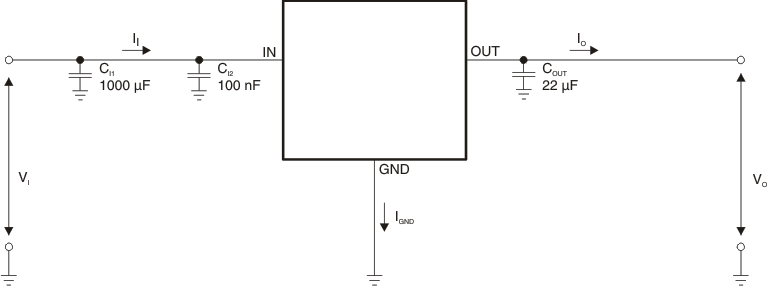
Parameter Measurement Information

TL720M05-Q1 Test
                    Circuit Figure 6-1 Test Circuit