SLVS028K April 1983 – September 2016 TL7702A , TL7705A , TL7709A , TL7712A , TL7715A
PRODUCTION DATA.
- 1 Features
- 2 Applications
- 3 Description
- 4 Revision History
- 5 Pin Configuration and Functions
- 6 Specifications
- 7 Parameter Measurement Information
- 8 Detailed Description
- 9 Application and Implementation
- 10Power Supply Recommendations
- 11Layout
- 12Device and Documentation Support
- 13Mechanical, Packaging, and Orderable Information
Package Options
Refer to the PDF data sheet for device specific package drawings
Mechanical Data (Package|Pins)
- D|8
- P|8
- PS|8
Thermal pad, mechanical data (Package|Pins)
- PS|8
Orderable Information
11 Layout
11.1 Layout Guidelines
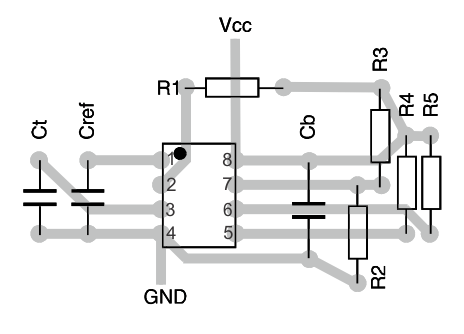
The voltage monitor should be placed on the printed circuit board, where there are no neighboring circuits in the which switch high currents (like bus interface circuits and power switches). When laying out the layout of the printed circuit board, take special care with the interconnects which carry analog signals. Beside the SENSE input these are the CT and Vref terminals. Noise coupled into the CT input will lead to a reduction of the output pulse width. Noise coupled into the Vref input or into the filter capacitor at this input may lead to undesired triggering of the circuit and by this to an undesired RESET pulse. Practice shows, that this malfunction when high currents flow over the interconnects of these capacitors to the GND terminal of the voltage monitor. To avoid these effects, the GND terminals of these capacitors must be connected by the shortest way to the GND terminal of the voltage monitor in so that no currents caused by other circuits flow over these wires. Figure 16 show a layout proposal for the printed circuit board. Furthermore the resistors of the voltage divider at the SENSE input of the TL7702 (R2 and R3 in Figure 16) have to be placed in so, that no noise may be coupled into this circuit.
11.2 Layout Example
 Figure 16. Printed Circuit Layout for the Supply Voltage Supervisor