SLVS037O September 1989 – December 2020 TL7702B , TL7705B , TL7733B
PRODUCTION DATA
- 1 Features
- 2 Applications
- 3 Description
- 4 Revision History
- 5 Pin Configuration and Functions
- 6 Specifications
- 7 Parameter Measurement Information
- 8 Detailed Description
- 9 Application and Implementation
- 10Power Supply Recommendations
- 11Layout
- 12Device and Documentation Support
- 13Mechanical, Packaging, and Orderable Information
Package Options
Refer to the PDF data sheet for device specific package drawings
Mechanical Data (Package|Pins)
- D|8
- P|8
Thermal pad, mechanical data (Package|Pins)
Orderable Information
10 Power Supply Recommendations
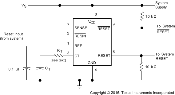
 Figure 10-1 System Reset Controller
With Undervoltage Sensing
Figure 10-1 System Reset Controller
With Undervoltage SensingWhen the TL770xB SENSE terminal is used to monitor VCC, TI recommends a current-limiting resistor in series with CT. During normal operation, the timing capacitor is charged by the onboard current source to approximately VCC or an internal voltage clamp (≈7.1-V Zener), whichever is less. When the circuit then is subjected to an undervoltage condition during which VCC is rapidly slewed down, the voltage on CT exceeds that on VCC. This forward biases a secondary path internally, which falsely activates the outputs. A fault is indicated when VCC drops below V(CT), not when VSENSE falls below VT–.
Adding the external resistor, RT, prevents false triggering. Its value is calculated as follows:
where
- V(CT) = VCC or 7.1 V, whichever is less
- VT– = 4.55 V (nom)
- RT = value of series resistor required
For VCC = 5 V
Therefore,
Using a 20%-tolerance resistor, RT should be greater than 560 Ω.
Adding this series resistor changes the duration of the reset pulse by no more than 10%. RT extends the discharge of CT, but also skews the V(CT) threshold. These effects tend to cancel one another. The precise percentage change can be derived theoretically, but the equation is complicated by this interaction and is dependent upon the duration of the supply-voltage fault condition.
Both outputs of the TL770xB must be terminated with similar value resistors, even when only one is being used. This prevents unwanted plateauing in either output waveform during switching, which may be interpreted as an undefined state or delay system reset.