SBAS980B June   2019  – June 2020 TLA2518

PRODUCTION DATA.  

  1. Features
  2. Applications
  3. Description
    1.     Device Images
      1.      TLA2518 Block Diagram and Applications
  4. Revision History
  5. Pin Configuration and Functions
    1.     Pin Functions
  6. Specifications
    1. 6.1 Absolute Maximum Ratings
    2. 6.2 ESD Ratings
    3. 6.3 Recommended Operating Conditions
    4. 6.4 Thermal Information
    5. 6.5 Electrical Characteristics
    6. 6.6 Timing Requirements
    7. 6.7 Switching Characteristics
    8. 6.8 Typical Characteristics
  7. Detailed Description
    1. 7.1 Overview
    2. 7.2 Functional Block Diagram
    3. 7.3 Feature Description
      1. 7.3.1 Multiplexer and ADC
      2. 7.3.2 Reference
      3. 7.3.3 ADC Transfer Function
      4. 7.3.4 ADC Offset Calibration
      5. 7.3.5 Programmable Averaging Filter
      6. 7.3.6 General-Purpose I/Os
      7. 7.3.7 Oscillator and Timing Control
      8. 7.3.8 Output Data Format
      9. 7.3.9 Device Programming
        1. 7.3.9.1 Enhanced-SPI Interface
        2. 7.3.9.2 Register Read/Write Operation
          1. 7.3.9.2.1 Register Write
          2. 7.3.9.2.2 Register Read
    4. 7.4 Device Functional Modes
      1. 7.4.1 Device Power-Up and Reset
      2. 7.4.2 Manual Mode
      3. 7.4.3 On-the-Fly Mode
      4. 7.4.4 Auto-Sequence Mode
    5. 7.5 TLA2518 Registers
      1. 7.5.1  SYSTEM_STATUS Register (Address = 0x0) [reset = 0x81]
        1. Table 9. SYSTEM_STATUS Register Field Descriptions
      2. 7.5.2  GENERAL_CFG Register (Address = 0x1) [reset = 0x0]
        1. Table 10. GENERAL_CFG Register Field Descriptions
      3. 7.5.3  DATA_CFG Register (Address = 0x2) [reset = 0x0]
        1. Table 11. DATA_CFG Register Field Descriptions
      4. 7.5.4  OSR_CFG Register (Address = 0x3) [reset = 0x0]
        1. Table 12. OSR_CFG Register Field Descriptions
      5. 7.5.5  OPMODE_CFG Register (Address = 0x4) [reset = 0x0]
        1. Table 13. OPMODE_CFG Register Field Descriptions
      6. 7.5.6  PIN_CFG Register (Address = 0x5) [reset = 0x0]
        1. Table 14. PIN_CFG Register Field Descriptions
      7. 7.5.7  GPIO_CFG Register (Address = 0x7) [reset = 0x0]
        1. Table 15. GPIO_CFG Register Field Descriptions
      8. 7.5.8  GPO_DRIVE_CFG Register (Address = 0x9) [reset = 0x0]
        1. Table 16. GPO_DRIVE_CFG Register Field Descriptions
      9. 7.5.9  GPO_VALUE Register (Address = 0xB) [reset = 0x0]
        1. Table 17. GPO_VALUE Register Field Descriptions
      10. 7.5.10 GPI_VALUE Register (Address = 0xD) [reset = 0x0]
        1. Table 18. GPI_VALUE Register Field Descriptions
      11. 7.5.11 SEQUENCE_CFG Register (Address = 0x10) [reset = 0x0]
        1. Table 19. SEQUENCE_CFG Register Field Descriptions
      12. 7.5.12 CHANNEL_SEL Register (Address = 0x11) [reset = 0x0]
        1. Table 20. CHANNEL_SEL Register Field Descriptions
      13. 7.5.13 AUTO_SEQ_CH_SEL Register (Address = 0x12) [reset = 0x0]
        1. Table 21. AUTO_SEQ_CH_SEL Register Field Descriptions
  8. Application and Implementation
    1. 8.1 Application Information
    2. 8.2 Typical Applications
      1. 8.2.1 Mixed-Channel Configuration
        1. 8.2.1.1 Design Requirements
        2. 8.2.1.2 Detailed Design Procedure
          1. 8.2.1.2.1 Digital Input
          2. 8.2.1.2.2 Digital Open-Drain Output
        3. 8.2.1.3 Application Curve
      2. 8.2.2 Digital Push-Pull Output Configuration
  9. Power Supply Recommendations
    1. 9.1 AVDD and DVDD Supply Recommendations
  10. 10Layout
    1. 10.1 Layout Guidelines
    2. 10.2 Layout Example
  11. 11Device and Documentation Support
    1. 11.1 Receiving Notification of Documentation Updates
    2. 11.2 Support Resources
    3. 11.3 Trademarks
    4. 11.4 Electrostatic Discharge Caution
    5. 11.5 Glossary
  12. 12Mechanical, Packaging, and Orderable Information

Package Options

Mechanical Data (Package|Pins)
Thermal pad, mechanical data (Package|Pins)
Orderable Information

Digital Open-Drain Output

The channels of the TLA2518 can be configured as digital open-drain outputs supporting an output voltage up to 5.5 V. An open-drain output, as shown in Figure 49, consists of an internal FET (Q) connected to ground. The output is idle when not driven by the device, which means Q is off and the pullup resistor, RPULL_UP, connects the GPOx node to the desired output voltage. The output voltage can range anywhere up to 5.5 V, depending on the external voltage that the GPIOx is pulled up to. When the device is driving the output, Q turns on, thus connecting the pullup resistor to ground and bringing the node voltage at GPOx low.
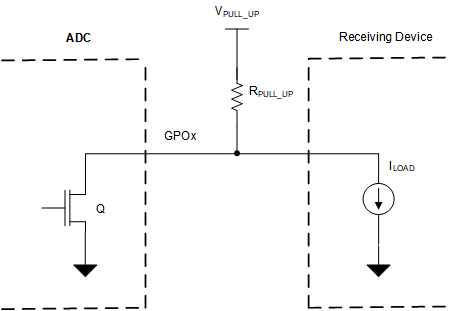
TLA2518 apps_digital_od_out.gifFigure 49. Digital Open-Drain Output

The minimum value of the pullup resistor, as calculated in Equation 3, is given by the ratio of VPULL_UP and the maximum current supported by the device digital output (5 mA).

Equation 3. RMIN = (VPULL_UP / 5 mA)

The maximum value of the pullup resistor, as calculated in Equation 4, depends on the minimum input current requirement, ILOAD, of the receiving device driven by this GPIO.

Equation 4. RMAX = (VPULL_UP / ILOAD)

Select RPULL_UP such that RMIN < RPULL_UP < RMAX.