SBAS980B
June 2019 – June 2020
TLA2518
PRODUCTION DATA.
1
Features
2
Applications
3
Description
Device Images
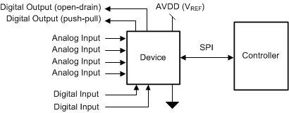
TLA2518 Block Diagram and Applications
4
Revision History
5
Pin Configuration and Functions
Pin Functions
6
Specifications
6.1
Absolute Maximum Ratings
6.2
ESD Ratings
6.3
Recommended Operating Conditions
6.4
Thermal Information
6.5
Electrical Characteristics
6.6
Timing Requirements
6.7
Switching Characteristics
6.8
Typical Characteristics
7
Detailed Description
7.1
Overview
7.2
Functional Block Diagram
7.3
Feature Description
7.3.1
Multiplexer and ADC
7.3.2
Reference
7.3.3
ADC Transfer Function
7.3.4
ADC Offset Calibration
7.3.5
Programmable Averaging Filter
7.3.6
General-Purpose I/Os
7.3.7
Oscillator and Timing Control
7.3.8
Output Data Format
7.3.9
Device Programming
7.3.9.1
Enhanced-SPI Interface
7.3.9.2
Register Read/Write Operation
7.3.9.2.1
Register Write
7.3.9.2.2
Register Read
7.4
Device Functional Modes
7.4.1
Device Power-Up and Reset
7.4.2
Manual Mode
7.4.3
On-the-Fly Mode
7.4.4
Auto-Sequence Mode
7.5
TLA2518 Registers
7.5.1
SYSTEM_STATUS Register (Address = 0x0) [reset = 0x81]
Table 9.
SYSTEM_STATUS Register Field Descriptions
7.5.2
GENERAL_CFG Register (Address = 0x1) [reset = 0x0]
Table 10.
GENERAL_CFG Register Field Descriptions
7.5.3
DATA_CFG Register (Address = 0x2) [reset = 0x0]
Table 11.
DATA_CFG Register Field Descriptions
7.5.4
OSR_CFG Register (Address = 0x3) [reset = 0x0]
Table 12.
OSR_CFG Register Field Descriptions
7.5.5
OPMODE_CFG Register (Address = 0x4) [reset = 0x0]
Table 13.
OPMODE_CFG Register Field Descriptions
7.5.6
PIN_CFG Register (Address = 0x5) [reset = 0x0]
Table 14.
PIN_CFG Register Field Descriptions
7.5.7
GPIO_CFG Register (Address = 0x7) [reset = 0x0]
Table 15.
GPIO_CFG Register Field Descriptions
7.5.8
GPO_DRIVE_CFG Register (Address = 0x9) [reset = 0x0]
Table 16.
GPO_DRIVE_CFG Register Field Descriptions
7.5.9
GPO_VALUE Register (Address = 0xB) [reset = 0x0]
Table 17.
GPO_VALUE Register Field Descriptions
7.5.10
GPI_VALUE Register (Address = 0xD) [reset = 0x0]
Table 18.
GPI_VALUE Register Field Descriptions
7.5.11
SEQUENCE_CFG Register (Address = 0x10) [reset = 0x0]
Table 19.
SEQUENCE_CFG Register Field Descriptions
7.5.12
CHANNEL_SEL Register (Address = 0x11) [reset = 0x0]
Table 20.
CHANNEL_SEL Register Field Descriptions
7.5.13
AUTO_SEQ_CH_SEL Register (Address = 0x12) [reset = 0x0]
Table 21.
AUTO_SEQ_CH_SEL Register Field Descriptions
8
Application and Implementation
8.1
Application Information
8.2
Typical Applications
8.2.1
Mixed-Channel Configuration
8.2.1.1
Design Requirements
8.2.1.2
Detailed Design Procedure
8.2.1.2.1
Digital Input
8.2.1.2.2
Digital Open-Drain Output
8.2.1.3
Application Curve
8.2.2
Digital Push-Pull Output Configuration
9
Power Supply Recommendations
9.1
AVDD and DVDD Supply Recommendations
10
Layout
10.1
Layout Guidelines
10.2
Layout Example
11
Device and Documentation Support
11.1
Receiving Notification of Documentation Updates
11.2
Support Resources
11.3
Trademarks
11.4
Electrostatic Discharge Caution
11.5
Glossary
12
Mechanical, Packaging, and Orderable Information
Package Options
Mechanical Data (Package|Pins)
RTE|16
MPQF149D
Thermal pad, mechanical data (Package|Pins)
RTE|16
QFND525B
Orderable Information
sbas980b_oa
sbas980b_pm
8.2.1
Mixed-Channel Configuration
Figure 47.
DAQ Circuit: Single-Supply DAQ