SNVSCR4 July   2024 TLA431

ADVANCE INFORMATION  

  1.   1
  2. Features
  3. Applications
  4. Description
  5. Device Comparison Table
  6. Pin Configuration and Functions
  7. Specifications
    1. 6.1 Absolute Maximum Ratings
    2. 6.2 ESD Ratings
    3. 6.3 Recommended Operating Conditions
    4. 6.4 Thermal Information
    5. 6.5 Electrical Characteristics
    6. 6.6 Typical Characteristics
  8. Parameter Measurement Information
    1. 7.1 Temperature Coefficient
    2. 7.2 Dynamic Impedance
  9. Detailed Description
    1. 8.1 Overview
    2. 8.2 Functional Block Diagram
    3. 8.3 Feature Description
    4. 8.4 Device Functional Modes
      1. 8.4.1 Closed Loop
      2. 8.4.2 Open Loop (Comparator)
  10. Applications and Implementation
    1. 9.1 Application Information
    2. 9.2 Typical Applications
      1. 9.2.1 Shunt Regulator/Reference
        1. 9.2.1.1 Design Requirements
        2. 9.2.1.2 Detailed Design Procedure
          1. 9.2.1.2.1 Programming Output/Cathode Voltage
          2. 9.2.1.2.2 Total Accuracy
          3. 9.2.1.2.3 Stability
          4. 9.2.1.2.4 Start-Up Time
        3. 9.2.1.3 Application Curve
      2. 9.2.2 Comparator With Integrated Reference
        1. 9.2.2.1 Design Requirements
        2. 9.2.2.2 Detailed Design Procedure
          1. 9.2.2.2.1 Basic Operation
            1. 9.2.2.2.1.1 Overdrive
          2. 9.2.2.2.2 Output Voltage and Logic Input Level
            1. 9.2.2.2.2.1 Input Resistance
        3. 9.2.2.3 Application Curve
    3. 9.3 System Examples
    4. 9.4 Power Supply Recommendations
    5. 9.5 Layout
      1. 9.5.1 Layout Guidelines
      2. 9.5.2 Layout Example
  11. 10Device and Documentation Support
    1. 10.1 Device Nomenclature
    2. 10.2 Related Links
    3. 10.3 Receiving Notification of Documentation Updates
    4. 10.4 Support Resources
    5. 10.5 Trademarks
    6. 10.6 Electrostatic Discharge Caution
    7. 10.7 Glossary
  12. 11Revision History
  13. 12Mechanical, Packaging, and Orderable Information

Package Options

Mechanical Data (Package|Pins)
Thermal pad, mechanical data (Package|Pins)

Temperature Coefficient

The deviation of the reference voltage, Vref, over the full temperature range is known as VI(dev). The parameter of VI(dev) can be used to find the temperature coefficient of the device. The average full-range temperature coefficient of the reference input voltage, αVref, is defined as:
TLA431 TLA432
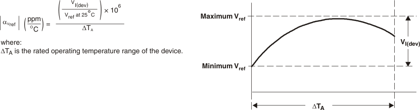
αVref is positive or negative, depending on whether minimum Vref or maximum Vref, respectively, occurs at the lower temperature. The full-range temperature coefficient is an average and therefore any subsection of the rated operating temperature range can yield a value that is greater or less than the average. For more details on temperature coefficient, refer to the Voltage Reference Selection Basics White Paper.