SLOS510E September 2006 – October 2016 TLC082-Q1 , TLC084-Q1
PRODUCTION DATA.
- 1 Features
- 2 Applications
- 3 Description
- 4 Revision History
- 5 Pin Configuration and Functions
-
6 Specifications
- 6.1 Absolute Maximum Ratings
- 6.2 ESD Ratings
- 6.3 Recommended Operating Conditions
- 6.4 Thermal Information
- 6.5 Electrical Characteristics: VDD = 5 V
- 6.6 Electrical Characteristics: VDD = 12 V
- 6.7 Operating Characteristics: VDD = 5 V
- 6.8 Operating Characteristics: VDD = 12 V
- 6.9 Typical Characteristics
- 7 Parameter Measurement Information
- 8 Detailed Description
- 9 Application and Implementation
- 10Power Supply Recommendations
- 11Layout
- 12Device and Documentation Support
- 13Mechanical, Packaging, and Orderable Information
Package Options
Mechanical Data (Package|Pins)
- DGN|8
Thermal pad, mechanical data (Package|Pins)
- DGN|8
Orderable Information
11 Layout
11.1 Layout Guidelines
To achieve the levels of high performance of the TLC08x-Q1, follow proper printed-circuit board (PCB) design techniques. A general set of guidelines is given in the following.
-
Ground planes TI highly recommends using a ground plane on the board to provide all components with a low-inductive ground connection. However, in the areas of the amplifier inputs and output, the ground plane can be removed to minimize the stray capacitance.
-
Proper power-supply decoupling Use a 6.8-μF tantalum capacitor in parallel with a 0.1-μF ceramic capacitor on each supply terminal. It may be possible to share the tantalum among several amplifiers depending on the application, but a 0.1-μF ceramic capacitor should always be used on the supply terminal of every amplifier. In addition, the 0.1-μF capacitor should be placed as close as possible to the supply terminal. As this distance increases, the inductance in the connecting trace makes the capacitor less effective. The designer should strive for distances of less than 0.1 inches between the device power terminals and the ceramic capacitors.
-
Sockets Sockets can be used but are not recommended. The additional lead inductance in the socket pins will often lead to stability problems. Surface-mount packages soldered directly to the PCB is the best implementation.
-
Short trace runs and compact part placements Optimum high performance is achieved when stray series inductance has been minimized. To realize this, the circuit layout should be made as compact as possible, thereby minimizing the length of all trace runs. Particular attention should be paid to the inverting input of the amplifier. Its length should be kept as short as possible. This helps minimize stray capacitance at the input of the amplifier.
-
Surface-mount passive components TI recommends using surface-mount passive components for high-performance amplifier circuits for several reasons. First, because of the extremely low lead inductance of surface-mount components, the problem with stray series inductance is greatly reduced. Second, the small size of surface-mount components naturally leads to a more-compact layout, thereby minimizing both stray inductance and capacitance. If leaded components are used, TI recommends keeping the lead lengths as short as possible.
11.1.1 General PowerPAD™ Design Considerations
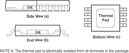
The TLC08x-Q1 is available in a thermally-enhanced PowerPAD family of packages. These packages are constructed using a downset leadframe upon which the die is mounted [see Figure 48(a) and Figure 48(b)]. This arrangement results in the lead frame being exposed as a thermal pad on the underside of the package [see Figure 48(c)]. Because this thermal pad has direct thermal contact with the die, excellent thermal performance can be achieved by providing a good thermal path away from the thermal pad.
 Figure 48. Views of Thermally-Enhanced DGN Package
The PowerPAD package allows for both assembly and thermal management in one manufacturing operation. During the surface-mount solder operation (when the leads are being soldered), the thermal pad must be soldered to a copper area underneath the package. Through the use of thermal paths within this copper area, heat can be conducted away from the package into either a ground plane or other heat dissipating device.
NOTE
Soldering the thermal pad to the PCB is always required, even with applications that have low power dissipation.
This soldering provides the necessary thermal and mechanical connection between the lead frame die pad and the PCB. Although there are many ways to properly heatsink the PowerPAD package, the following steps list the recommended approach.
The thermal pad must be connected to the most-negative supply voltage (GND pin potential) of the device.
- Prepare the PCB with a top-side etch pattern (see the landing patterns at the end of this data sheet). There should be etch for the leads, as well as etch for the thermal pad.
- Place five holes (dual) or nine holes (quad) in the area of the thermal pad. These holes should be 13 mils in diameter. Keep them small so that solder wicking through the holes is not a problem during reflow.
- Additional vias may be placed anywhere along the thermal plane outside of the thermal pad area. This helps dissipate the heat generated by the TLC08x-Q1 device. These additional vias may be larger than the 13-mil diameter vias directly under the thermal pad. They can be larger because they are not in the thermal-pad area to be soldered, so that wicking is not a problem.
- Connect all holes to the internal plane that is at the same potential as the ground pin of the device.
- When connecting these holes to this internal plane, do not use the typical web or spoke via connection methodology. Web connections have a high-thermal-resistance connection that is useful for slowing the heat transfer during soldering operations. This makes the soldering of vias that have plane connections easier. In this application, however, low thermal resistance is desired for the most efficient heat transfer. Therefore, the holes under the TLC08x-Q1 PowerPAD package should make their connection to the internal ground plane with a complete connection around the entire circumference of the plated-through hole.
- The top-side solder mask should leave the terminals of the package and the thermal-pad area with its five holes (dual) or nine holes (quad) exposed. The bottom-side solder mask should cover the five or nine holes of the thermal-pad area. This prevents solder from being pulled away from the thermal-pad area during the reflow process.
- Apply solder paste to the exposed thermal-pad area and all of the IC terminals.
- With these preparatory steps in place, the TLC08x-Q1 IC is simply placed in position and run through the solder reflow operation as any standard surface-mount component. This results in a part that is properly installed.
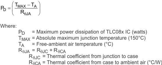
For a given RθJA, use Equation 1 to calculate the maximum power dissipation.

The next consideration is the package constraints. The two sources of heat within an amplifier are quiescent power and output power. The designer should never forget about the quiescent heat generated within the device, especially multi-amplifier devices. Because these devices have linear output stages (class A-B), most of the heat dissipation is at low-output voltages with high-output currents.
The other key factor when dealing with power dissipation is how the devices are mounted on the PCB. The PowerPAD devices are extremely useful for heat dissipation. But, the device should always be soldered to a copper plane to fully use the heat dissipation properties of the thermal pad. The SOIC package, on the other hand, is highly dependent on how it is mounted on the PCB. As more trace and copper area is placed around the device, RθJA decreases and the heat dissipation capability increases. The currents and voltages shown in Typical Characteristics are for the total package. For the dual or quad amplifier packages, the sum of the RMS output currents and voltages should be used to choose the proper package.
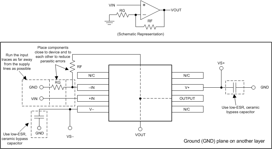
11.2 Layout Example
 Figure 49. Operational Amplifier Board Layout for Noninverting Configuration