SLOS510E September 2006 – October 2016 TLC082-Q1 , TLC084-Q1
PRODUCTION DATA.
- 1 Features
- 2 Applications
- 3 Description
- 4 Revision History
- 5 Pin Configuration and Functions
-
6 Specifications
- 6.1 Absolute Maximum Ratings
- 6.2 ESD Ratings
- 6.3 Recommended Operating Conditions
- 6.4 Thermal Information
- 6.5 Electrical Characteristics: VDD = 5 V
- 6.6 Electrical Characteristics: VDD = 12 V
- 6.7 Operating Characteristics: VDD = 5 V
- 6.8 Operating Characteristics: VDD = 12 V
- 6.9 Typical Characteristics
- 7 Parameter Measurement Information
- 8 Detailed Description
- 9 Application and Implementation
- 10Power Supply Recommendations
- 11Layout
- 12Device and Documentation Support
- 13Mechanical, Packaging, and Orderable Information
Package Options
Mechanical Data (Package|Pins)
- DGN|8
Thermal pad, mechanical data (Package|Pins)
- DGN|8
Orderable Information
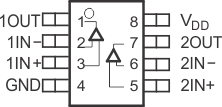
5 Pin Configuration and Functions
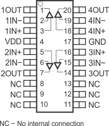
PWP Package
20-Pin HTSSOP
Top View

Pin Functions
| PIN | I/O | DESCRIPTION | ||
|---|---|---|---|---|
| NAME | NO. | |||
| TLC082-Q1 | TLC084-Q1 | |||
| 1IN+ | 3 | 3 | I | Noninverting input, Channel 1 |
| 1IN– | 2 | 2 | I | Inverting input, Channel 1 |
| 1OUT | 1 | 1 | O | Output, Channel 1 |
| 2IN+ | 5 | 5 | I | Noninverting input, Channel 2 |
| 2IN– | 6 | 6 | I | Inverting input, Channel 2 |
| 2OUT | 7 | 7 | O | Output, Channel 2 |
| 3IN+ | — | 16 | I | Noninverting input, Channel 3 |
| 3IN– | — | 15 | I | Inverting input, Channel 3 |
| 3OUT | — | 14 | O | Output, Channel 3 |
| 4IN+ | — | 18 | I | Noninverting input, Channel 4 |
| 4IN– | — | 19 | I | Inverting input, Channel 4 |
| 4OUT | — | 20 | O | Output, Channel 4 |
| GND | 4 | 17 | — | Negative (lowest) power supply |
| NC | — | 8 to13 | — | Non-connect |
| VDD | 8 | 4 | I | Positive (highest) power supply |
