SLOS510E September 2006 – October 2016 TLC082-Q1 , TLC084-Q1
PRODUCTION DATA.
- 1 Features
- 2 Applications
- 3 Description
- 4 Revision History
- 5 Pin Configuration and Functions
-
6 Specifications
- 6.1 Absolute Maximum Ratings
- 6.2 ESD Ratings
- 6.3 Recommended Operating Conditions
- 6.4 Thermal Information
- 6.5 Electrical Characteristics: VDD = 5 V
- 6.6 Electrical Characteristics: VDD = 12 V
- 6.7 Operating Characteristics: VDD = 5 V
- 6.8 Operating Characteristics: VDD = 12 V
- 6.9 Typical Characteristics
- 7 Parameter Measurement Information
- 8 Detailed Description
- 9 Application and Implementation
- 10Power Supply Recommendations
- 11Layout
- 12Device and Documentation Support
- 13Mechanical, Packaging, and Orderable Information
Package Options
Mechanical Data (Package|Pins)
- PWP|20
Thermal pad, mechanical data (Package|Pins)
- PWP|20
Orderable Information
9 Application and Implementation
NOTE
Information in the following applications sections is not part of the TI component specification, and TI does not warrant its accuracy or completeness. TI’s customers are responsible for determining suitability of components for their purposes. Customers should validate and test their design implementation to confirm system functionality.
9.1 Application Information
The TLC08x-Q1 devices features wide supply voltage range, high-output current drive in the order of 60 mA, low input offset voltage, a high unity gain bandwidth 10 MHz and high slew of 16 V/µS. These features make the device suitable in amplifying high-frequency and slew rate signals.
9.2 Typical Applications
9.2.1 TLC08x-Q1 Single-Supply Typical Application
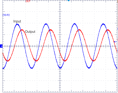
Some applications require amplification of low amplitude and relatively high-frequency input signal. The sine wave maximum slew rate is at zero crossing. The amplified signal distorts if the minimum slew rate is not met. Operational amplifier slew rate must be higher than 2 × π × F × V, where F is the input signal frequency and V is the output signal amplitude. TLC08x-Q1 Slew rate of 16 V/µS is capable of delivering an output signal of 2-V peak and 1-MHz frequency with no distortion. See Figure 45 for an application curve that shows the results of Figure 39.
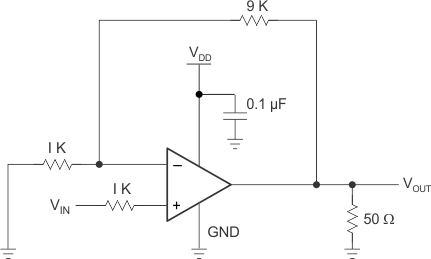 Figure 39. TLC08x-Q1 Typical Application
9.2.1.1 Design Requirements
Use the following parameters for this design example:
- Noninverting configuration with gain of 10 or 20 dB
- Single supply minimum: 4.5 V
- Single supply maximum: 16 V
- Output common mode minimum should be higher than output level VOL
- Output common mode maximum should be lower than output level VOH
- Unity gain bandwidth: 10 MHz
- Output load current lower than 60 mA
- Maximum input signal frequency below 1 MHz for less than –3-dB attenuation at 1 MHz
9.2.1.2 Detailed Design Procedure
9.2.1.2.1 Driving a Capacitive Load
When the amplifier is configured in this manner, capacitive loading directly on the output decreases the device phase margin, leading to high-frequency ringing or oscillations. Therefore, for capacitive loads of greater than
10 pF, TI recommends placing a resistor in series (RNULL) with the output of the amplifier, as shown in Figure 40. A minimum value of 20 Ω should work well for most applications.
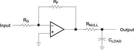 Figure 40. Driving a Capacitive Load
9.2.1.2.2 Offset Voltage
The output offset voltage, (VOO) is the sum of the input offset voltage (VIO) and both input bias currents (IIB) times the corresponding gains. The schematic and formula in Figure 41 can be used to calculate the output offset voltage.
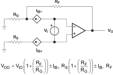 Figure 41. Output Offset Voltage Model
9.2.1.2.3 High-Speed CMOS Input Amplifiers
The TLC08x-Q1 is a family of high-speed low-noise CMOS input operational amplifiers that has an input capacitance on the order of 20 pF. Any resistor used in the feedback path adds a pole in the transfer function equivalent to the input capacitance multiplied by the combination of source resistance and feedback resistance. For example, a gain of –10, a source resistance of 1 kΩ, and a feedback resistance of 10 kΩ add an additional pole at approximately 8 MHz. This is more apparent with CMOS amplifiers than bipolar amplifiers due to their greater input capacitance.
This is of little consequence on slower CMOS amplifiers, as this pole normally occurs at frequencies above their unity-gain bandwidth. However, the TLC08x-Q1 with its 10-MHz bandwidth means that this pole normally occurs at frequencies where there is on the order of 5-dB gain left and the phase shift adds considerably.
The effect of this pole is the strongest with large feedback resistances at small closed-loop gains. As the feedback resistance is increased, the gain peaking increases at a lower frequency and the 180° phase-shift crossover point also moves down in frequency, decreasing the phase margin.
For the TLC08x-Q1, the maximum feedback resistor recommended is 5 kΩ; larger resistances can be used but a capacitor in parallel with the feedback resistor is recommended to counter the effects of the input capacitance pole.
The TLC08x-Q1 with a 1-V step response has an 80% overshoot with a natural frequency of 3.5 MHz when configured as a unity gain buffer and with a 10-kΩ feedback resistor. By adding a 10-pF capacitor in parallel with the feedback resistor, the overshoot is reduced to 40% and eliminates the natural frequency, resulting in a much faster settling time (see Figure 42). The 10-pF capacitor was chosen for convenience only.
Load capacitance had little effect on these measurements due to the excellent output drive capability of the TLC08x-Q1.
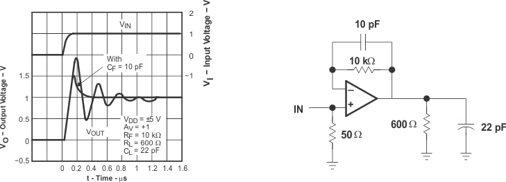 Figure 42. 1-V Step Response
9.2.1.2.4 General Configurations
When receiving low-level signals, limiting the bandwidth of the incoming signals into the system is often required. The simplest way to accomplish this is to place an RC filter at the noninverting terminal of the amplifier (see Figure 43).
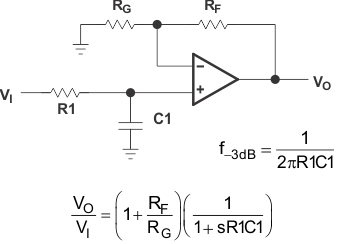 Figure 43. Single-Pole Low-Pass Filter
If even more attenuation is needed, a multiple-pole filter is required. The Sallen-Key filter can be used for this task. For best results, the amplifier should have a bandwidth that is eight to ten times the filter frequency bandwidth. Failure to do this can result in phase shift of the amplifier.
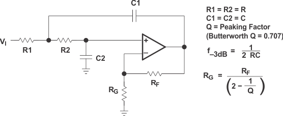 Figure 44. 2-Pole Low-Pass Sallen-Key Filter
9.2.1.3 Application Curve
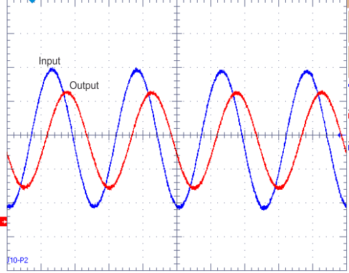
| Gain Vout / Vin = 1.471 V / 0.2 V = 7.335 | ||
| Gain(db) = 20 Log (7.335) = 17.33 dB and is 2.7 dB below 10 dB |
||
9.2.2 Dual-Supply Typical Application
The dual-supply application has a gain of 10 and a bandwidth of 1 MHz.
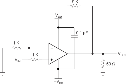 Figure 46. Dual Supply Typical Application Schematic
9.2.2.1 Design Requirements
Use the following parameters for this design example:
- Noninverting configuration with gain of 10 or 20 dB
- Dual supply minimum: ±2.25 V
- Dual supply maximum: ±8 V
- Output common mode minimum should be higher than output level VOL
- Output common mode maximum should be lower than output level VOH
- Unity gain bandwidth: 10 MHz
- Maximum input signal frequency is 1 MHz for less than 3-dB attenuation at 1 MHz
- Output load current lower than 60 mA
9.2.2.2 Detailed Design Procedure
For this example, see Detailed Design Procedure in TLC08x-Q1 Single-Supply Typical Application.
9.2.2.3 Application Curve
