SGLS007G February 2003 – August 2022 TLC2272-Q1 , TLC2272A-Q1 , TLC2274-Q1 , TLC2274A-Q1
PRODUCTION DATA
- 1 Features
- 2 Applications
- 3 Description
- 4 Revision History
- 5 Pin Configuration and Functions
-
6 Specifications
- 6.1 Absolute Maximum Ratings
- 6.2 ESD Ratings
- 6.3 Recommended Operating Conditions
- 6.4 Thermal Information
- 6.5 Electrical Characteristics: VDD = 5 V (TLC2272-Q1 and TLC2272A-Q1)
- 6.6 Electrical Characteristics: VDD± = ±5 V (TLC2272-Q1 and TLC2272A-Q1)
- 6.7 Electrical Characteristics: VDD = 5 V (TLC2274-Q1 and TLC2274A-Q1)
- 6.8 Electrical Characteristics: VDD± = ±5 V (TLC2274-Q1 and TLC2274A-Q1)
- 6.9 Typical Characteristics
- 7 Detailed Description
- 8 Application and Implementation
- 9 Device and Documentation Support
- 10Mechanical, Packaging, and Orderable Information
Package Options
Mechanical Data (Package|Pins)
Thermal pad, mechanical data (Package|Pins)
Orderable Information
6.9 Typical Characteristics
Table 6-1 Table of Graphs
| FIGURE(1) | |||
|---|---|---|---|
| VIO | Input offset voltage | Distribution | 1, 2, 3, 4 |
| vs Common-mode voltage | 5, 6 | ||
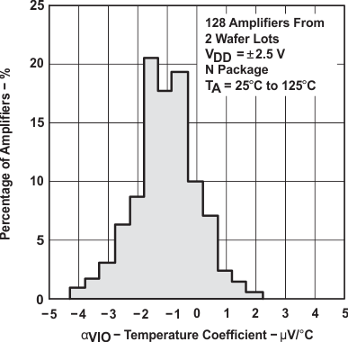
| αVIO | Input offset voltage temperature coefficient | Distribution | 7, 8, 9, 10(2) |
| IIB /IIO | Input bias and input offset current | vs Free-air temperature | 11(2) |
| VI | Input voltage | vs Supply voltage | 12 |
| vs Free-air temperature | 13(2) | ||
| VOH | High-level output voltage | vs High-level output current | 14(2) |
| VOL | Low-level output voltage | vs Low-level output current | 15, 16(2) |
| VOM+ | Maximum positive peak output voltage | vs Output current | 17(2) |
| VOM- | Maximum negative peak output voltage | vs Output current | 18(2) |
| VO(PP) | Maximum peak-to-peak output voltage | vs Frequency | 19 |
| IOS | Short-circuit output current | vs Supply voltage | 20 |
| vs Free-air temperature | 21(2) | ||
| VO | Output voltage | vs Differential input voltage | 22, 23 |
| AVD | Large-signal differential voltage amplification | vs Load resistance | 24 |
| Large-signal differential voltage amplification and phase margin | vs Frequency | 25, 26 | |
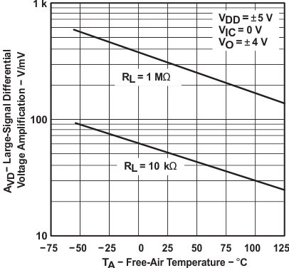
| Large-signal differential voltage amplification | vs Free-air temperature | 27(2), 28(2) | |
| z0 | Output impedance | vs Frequency | 29, 30 |
| CMRR | Common-mode rejection ratio | vs Frequency | 31 |
| vs Free-air temperature | 32 | ||
| kSVR | Supply-voltage rejection ratio | vs Frequency | 33, 34 |
| vs Free-air temperature | 35(2) | ||
| IDD | Supply current | vs Supply voltage | 36(2), 37(2) |
| vs Free-air temperature | 38(2), 39(2) | ||
| SR | Slew rate | vs Load Capacitance | 40 |
| vs Free-air temperature | 41(2) | ||
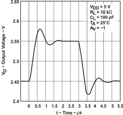
| VO | Inverting large-signal pulse response | 42, 43 | |
| Voltage-follower large-signal pulse response | 44, 45 | ||
| Inverting small-signal pulse response | 46, 47 | ||
| Voltage-follower small-signal pulse response | 48, 49 | ||
| Vn | Equivalent input noise voltage | vs Frequency | 50, 51 |
| Noise voltage over a 10-second period | 52 | ||
| Integrated noise voltage | vs Frequency | 53 | |
| THD+N | Total harmonic distortion + noise | vs Frequency | 54 |
| Gain-bandwidth product | vs Supply voltage | 55 | |
| vs Free-air temperature | 56(2) | ||
| φm | Phase margin | vs Load capacitance | 57 |
| Gain margin | vs Load capacitance | 58 | |
(1) For all graphs where VDD = 5 V, all loads are referenced to 2.5 V.
(2) Data at high and low temperatures are applicable only within the rated operating free-air temperature ranges of the various devices.
 Figure 6-1 Distribution of TLC2272-Q1 Input Offset Voltage
 Figure 6-3 Distribution of TLC2274-Q1 Input Offset Voltage
 Figure 6-5 Input Offset Voltage vs Common-Mode Voltage
 Figure 6-7 Distribution of TLC2272-Q1 vs Input Offset Voltage Temperature Coefficient
 Figure 6-9 Distribution of TLC2274-Q1 vs Input Offset Voltage Temperature Coefficient
 Figure 6-11 Input Bias and Input Offset Current vs Free-Air Temperature
 Figure 6-13 Input Voltage vs Free-Air Temperature
 Figure 6-15 Low-Level Output Voltage vs Low-Level Output Current
 Figure 6-17 Maximum Positive Peak Output Voltage vs Output Current
 Figure 6-19 Maximum Peak-to-Peak Output Voltage vs Frequency
 Figure 6-21 Short-Circuit Output Current vs Free-Air Temperature
 Figure 6-23 Output Voltage vs Differential Input Voltage
 Figure 6-25 Large-Signal Differential Voltage Amplification and Phase Margin vs Frequency
 Figure 6-27 Large-Signal Differential Voltage Amplification vs Free-Air Temperature
 Figure 6-29 Output Impedance vs Frequency
 Figure 6-31 Common-Mode Rejection Ratio vs Frequency
 Figure 6-33 Supply-Voltage Rejection Ratio vs Frequency
 Figure 6-35 Supply-Voltage Rejection Ratio vs Free-Air Temperature
 Figure 6-37 TLC2274-Q1 Supply Current vs Supply Voltage
 Figure 6-39 TLC2274-Q1 Supply Current vs Free-Air Temperature
 Figure 6-41 Slew Rate vs Free-Air Temperature
 Figure 6-43 Inverting Large-Signal Pulse Response
 Figure 6-45 Voltage-Follower Large-Signal Pulse Response
 Figure 6-47 Inverting Small-Signal Pulse Response
 Figure 6-49 Voltage-Follower Small-Signal Pulse Response
 Figure 6-51 Equivalent Input Noise Voltage vs Frequency
 Figure 6-53 Integrated Noise Voltage vs Frequency
 Figure 6-55 Gain-Bandwidth Product vs Supply Voltage
 Figure 6-57 Phase Margin vs Load Capacitance
 Figure 6-2 Distribution of TLC2272-Q1 Input Offset Voltage
 Figure 6-4 Distribution of TLC2274-Q1 Input Offset Voltage
 Figure 6-6 Input Offset Voltage vs Common-Mode Voltage
 Figure 6-8 Distribution of TLC2272-Q1 vs Input Offset Voltage Temperature Coefficient
 Figure 6-10 Distribution of TLC2274-Q1 vs Input Offset Voltage Temperature Coefficient
 Figure 6-12 Input Voltage vs Supply Voltage
 Figure 6-14 High-Level Output Voltage vs High-Level Output Current
 Figure 6-16 Low-Level Output Voltage vs Low-Level Output Current
 Figure 6-18 Maximum Positive Peak Output Voltage vs Output Current
 Figure 6-20 Short-Circuit Output Current vs Supply Voltage
 Figure 6-22 Output Voltage vs Differential Input Voltage
 Figure 6-24 Large-Signal Differential Voltage Amplification vs Load Resistance
 Figure 6-26 Large-Signal Differential Voltage Amplification and Phase Margin vs Frequency
 Figure 6-28 Large-Signal Differential Voltage Amplification vs Free-Air Temperature
 Figure 6-30 Output Impedance vs Frequency
 Figure 6-32 Common-Mode Rejection Ratio vs Free-Air Temperature
 Figure 6-34 Supply-Voltage Rejection Ratio vs Frequency
 Figure 6-36 TLC2272-Q1 Supply Current vs Supply Voltage
 Figure 6-38 TLC2272-Q1 Supply Current vs Free-Air Temperature
 Figure 6-40 Slew Rate vs Load Capacitance
 Figure 6-42 Inverting Large-Signal Pulse Response
 Figure 6-44 Voltage-Follower Large-Signal Pulse Response
 Figure 6-46 Inverting Small-Signal Pulse Response
 Figure 6-48 Voltage-Follower Small-Signal Pulse Response
 Figure 6-50 Equivalent Input Noise Voltage vs Frequency
 Figure 6-52 Noise Voltage Over a 10 Second Period
 Figure 6-54 Total Harmonic Distortion + Noise vs Frequency
 Figure 6-56 Gain-Bandwidth Product vs Free-Air Temperature
 Figure 6-58 Gain Margin vs Load Capacitance