SLOS190H February 1997 – March 2016 TLC2272 , TLC2272A , TLC2272AM , TLC2272M , TLC2274 , TLC2274A , TLC2274AM
PRODUCTION DATA.
- 1 Features
- 2 Applications
- 3 Description
- 4 Revision History
- 5 Pin Configuration and Functions
-
6 Specifications
- 6.1 Absolute Maximum Ratings
- 6.2 ESD Ratings
- 6.3 Recommended Operating Conditions
- 6.4 Thermal Information
- 6.5 TLC2272 and TLC2272A Electrical Characteristics VDD = 5 V
- 6.6 TLC2272 and TLC2272A Electrical Characteristics VDD± = ±5 V
- 6.7 TLC2274 and TLC2274A Electrical Characteristics VDD = 5 V
- 6.8 TLC2274 and TLC2274A Electrical Characteristics VDD± = ±5 V
- 6.9 Typical Characteristics
- 7 Detailed Description
- 8 Application and Implementation
- 9 Power Supply Recommendations
- 10Layout
- 11Device and Documentation Support
- 12Mechanical, Packaging, and Orderable Information
Package Options
Mechanical Data (Package|Pins)
- D|14
Thermal pad, mechanical data (Package|Pins)
Orderable Information
10 Layout
10.1 Layout Guidelines
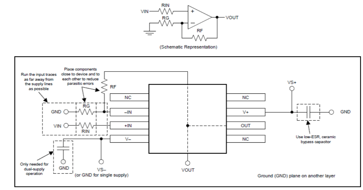
The TLC227x and TLC227xA families of devices are wideband amplifiers. To realize the full operational performance of the devices, good high-frequency printed-circuit-board (PCB) layout practices are required. Low-loss 0.1-μF bypass capacitors must be connected between each supply pin and ground as close to the device as possible. The bypass capacitor traces should be designed for minimum inductance.
10.2 Layout Example
 Figure 63. Layout Example