SLOS985 June 2017 TLC2274M-MIL
PRODUCTION DATA.
- 1 Features
- 2 Applications
- 3 Description
- 4 Revision History
- 5 Pin Configuration and Functions
- 6 Specifications
- 7 Detailed Description
- 8 Application and Implementation
- 9 Power Supply Recommendations
- 10Layout
- 11Device and Documentation Support
- 12Mechanical, Packaging, and Orderable Information
Package Options
Mechanical Data (Package|Pins)
Thermal pad, mechanical data (Package|Pins)
Orderable Information
8 Application and Implementation
NOTE
Information in the following applications sections is not part of the TI component specification, and TI does not warrant its accuracy or completeness. TI’s customers are responsible for determining suitability of components for their purposes. Customers should validate and test their design implementation to confirm system functionality.
8.1 Application Information
8.1.1 Macromodel Information
Macromodel information provided was derived using MicroSim Parts™, the model generation software used with MicroSim PSpice™. The Boyle macromodel , IEEE Journal of Solid-State Circuits, SC-9, 353 (1974). and subcircuit in Figure 53 were generated using the TLC2274M-MIL typical electrical and operating characteristics at TA = 25°C. Using this information, output simulations of the following key parameters can be generated to a tolerance of 20% (in most cases):
- Maximum positive output voltage swing
- Maximum negative output voltage swing
- Slew rate
- Quiescent power dissipation
- Input bias current
- Open-loop voltage amplification
- Unity-gain frequency
- Common-mode rejection ratio
- Phase margin
- DC output resistance
- AC output resistance
- Short-circuit output current limit
 Figure 53. Boyle Macromodel and Subcircuit
8.2 Typical Application
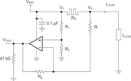
8.2.1 High-Side Current Monitor
 Figure 54. Equivalent Schematic (Each Amplifier)
8.2.1.1 Design Requirements
For this design example, use the parameters listed in Table 3 as the input parameters.
Table 3. Design Parameters
| PARAMETER | VALUE | |
|---|---|---|
| VBAT | Battery voltage | 12 V |
| RSENSE | Sense resistor | 0.1 Ω |
| ILOAD | Load current | 0 A to 10 A |
| Operational amplifier | Set in differential configuration with gain = 10 | |
8.2.1.2 Detailed Design Procedure
This circuit is designed for measuring the high-side current in automotive body control modules with a 12-V battery or similar applications. The operational amplifier is set as differential with an external resistor network.
8.2.1.2.1 Differential Amplifier Equations
Equation 1 and Equation 2 are used to calculate VOUT.


In an ideal case R1 = R and R2 = Rg, and VOUT can then be calculated using Equation 3:

However, as the resistors have tolerances, they cannot be perfectly matched.
R1 = R ± ΔR1
R2 = R2 ± ΔR2
R = R ± ΔR
Rg = Rg ± ΔRg

By developing the equations and neglecting the second order, the worst case is when the tolerances add up. This is shown by Equation 5.

where
- Tol = 0.01 for 1%
- Tol = 0.001 for 0.1%
If the resistors are perfectly matched, then Tol = 0 and VOUT is calculated using Equation 6.

The highest error is from the common mode, as shown in Equation 7.

Gain of 10, Rg / R = 10, and Tol = 1%:
Common mode error = ((4 × 0.01) / 1.1) × 12 V = 0.436 V
Gain of 10 and Tol = 0.1%:
Common mode error = 43.6 mV
The resistors were chosen from 2% batches.
R1 and R 12 kΩ
R2 and Rg 120 kΩ
Ideal Gain = 120 / 12 = 10
The measured value of the resistors:
R1 = 11.835 kΩ
R = 11.85 kΩ
R2 = 117.92 kΩ
Rg = 118.07 kΩ
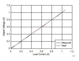
8.2.1.3 Application Curves
 Figure 55. Output Voltage Measured vs Ideal
(0 to 1 A)
 Figure 56. Output Voltage Measured vs Ideal
(0 to 10 A)