SLFS083A July 2024 – October 2024 TLC3555-Q1
PRODMIX
- 1
- 1 Features
- 2 Applications
- 3 Description
- 4 Pin Configuration and Functions
- 5 Specifications
- 6 Detailed Description
- 7 Application and Implementation
- 8 Device and Documentation Support
- 9 Revision History
- 10Mechanical, Packaging, and Orderable Information
Package Options
Refer to the PDF data sheet for device specific package drawings
Mechanical Data (Package|Pins)
- D|8
- DDF|8
Thermal pad, mechanical data (Package|Pins)
Orderable Information
6.3.1 Monostable Operation
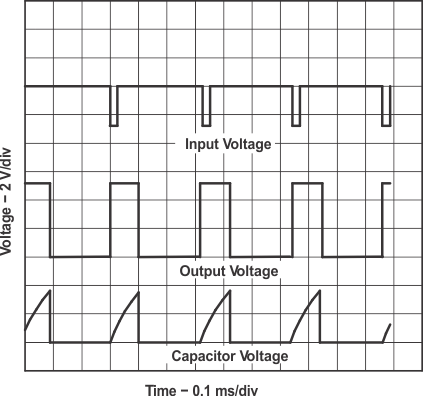
For monostable operation, connect the TLC3555-Q1 as in Figure 6-1. If the output is low, application of a negative-going pulse to the trigger (TRIG) sets the internal flip-flop, drives the output high, and turns off DISCH. Capacitor CT charges through RA until the voltage across the capacitor reaches the threshold voltage of the threshold (THRES) input. If TRIG returns to a high level, the output of the threshold comparator resets the flip-flop, drives the output low, and discharges CT through DISCH.
 Figure 6-1 Circuit
for Monostable Operation
Figure 6-1 Circuit
for Monostable OperationMonostable operation initiates when the TRIG voltage is less than the trigger threshold. After initialization, the sequence ends only if TRIG is high for at least 500ns before the end of the timing interval. When the trigger is grounded, the comparator storage time can be as long as 500ns, which limits the minimum monostable pulse width to 500ns. As a result of the threshold level and saturation voltage of the discharge transistor, the output pulse duration is approximately tw = 1.1 × RA × CT. Figure 6-3 is a plot of the nominal pulse width for various values of RA and CT. The threshold levels and charge rates are directly proportional to the supply voltage (VDD). As a result, the timing interval is independent of the supply voltage if the supply voltage is constant during the time interval.
Apply a negative-going trigger pulse simultaneously to RESET and TRIG during the timing interval to discharge CT and reinitiate the cycle, commencing on the positive edge of the reset pulse. The output is held low for as long as the reset pulse is low.

| RA = 9.1kΩ | CT = 0.01µF |
