SLDS162B March 2009 – December 2015 TLC59108F
PRODUCTION DATA.
- 1 Features
- 2 Applications
- 3 Description
- 4 Revision History
- 5 Pin Configuration and Functions
- 6 Specifications
- 7 Parameter Measurement Information
-
8 Detailed Description
- 8.1 Overview
- 8.2 Functional Block Diagram
- 8.3 Feature Description
- 8.4 Device Functional Modes
- 8.5 Programming
- 8.6
Register Maps
- 8.6.1 Control Register
- 8.6.2 Mode Register 1 (MODE1)
- 8.6.3 Mode Register 2 (MODE2)
- 8.6.4 Individual Brightness Control Registers (PWM0-PWM7)
- 8.6.5 Group Duty Cycle Control Register (GRPPWM)
- 8.6.6 Group Frequency Register (GRPFREQ)
- 8.6.7 LED Driver Output State Registers (LEDOUT0, LEDOUT1)
- 8.6.8 I2C Bus Sub-Address Registers 1 to 3 (SUBADR1-SUBADR3)
- 8.6.9 LED All Call I2C Bus Address Register (ALLCALLADR)
- 9 Application and Implementation
- 10Power Supply Recommendations
- 11Layout
- 12Device and Documentation Support
- 13Mechanical, Packaging, and Orderable Information
Package Options
Mechanical Data (Package|Pins)
- PW|20
Thermal pad, mechanical data (Package|Pins)
Orderable Information
9 Application and Implementation
NOTE
Information in the following applications sections is not part of the TI component specification, and TI does not warrant its accuracy or completeness. TI’s customers are responsible for determining suitability of components for their purposes. Customers should validate and test their design implementation to confirm system functionality.
9.1 Application Information
9.1.1 Setting LED Current
The LED current is primarily dependent on the supply voltage, the forward voltage of the LED, and the series resistor (RSET). In many applications the supply voltage and LED forward voltage cannot be adjusted. Hence, RSET is used to adjust the LED current. This calculation is discussed in detail in the typical application example.
9.1.2 PWM Brightness Dimming
The perceived brightness of the LEDs can be adjusted by use of PWM dimming. For example, an LED driven at 50% duty cycle will appear less bright than it would at 100% duty cycle. The TLC59116F offers duty cycle control for each individual channel and also offers group duty cycle control. Refer to the Register Maps for details regarding programmable duty cycle.
9.1.3 TLC59108 and TLC59108F Differences
The TLC59108 and TLC59108F are similar devices with the difference being the output structure. The TLC59108 has 8 constant-current outputs while the TLC59108F has 8 open-drain outputs. The REXT is used to program the current on the TLC59108 for all channels. The in-line resistors on the OUT pins are used in conjunction with the VLED to set the currents on each TLC59108F channel. Because the resistors are unique for each output, the currents can be set by output by changing the resistor value.
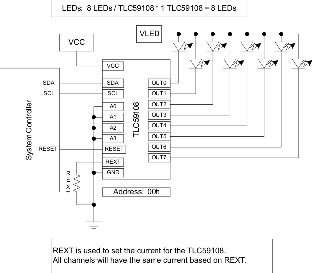 Figure 20. TLC59108 One Driver
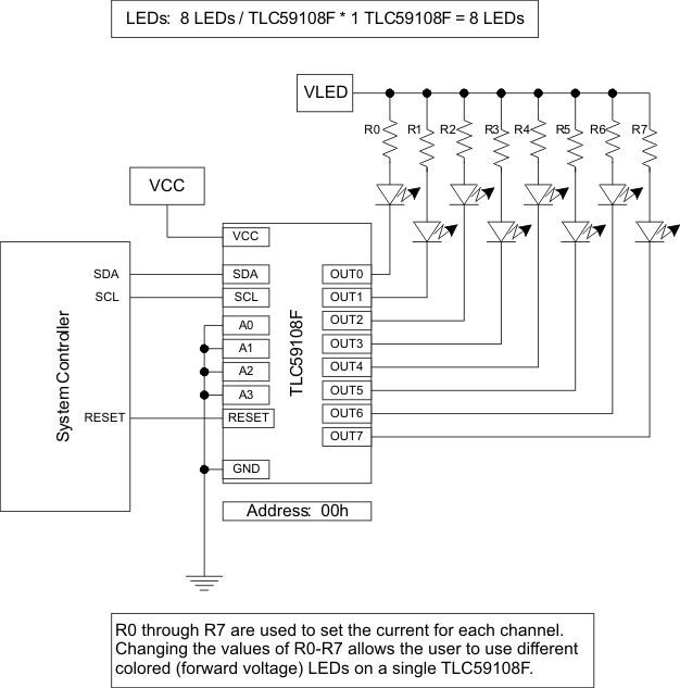 Figure 21. TLC59108F One Driver
9.1.4 Connecting Multiple Devices
This drawing is an example of using the TLC59108F in a system requiring up to 48 LED strings. The TLC59108F drivers share a single I2C bus. The address pins are set high or low to enable the drivers to be independently accessed (all can be written in parallel through the ALLCALLADR function). The resistors in series with the LEDs along with the VLED voltage will set the current for each string independently. Changing the resistor values allows for multi-color displays.
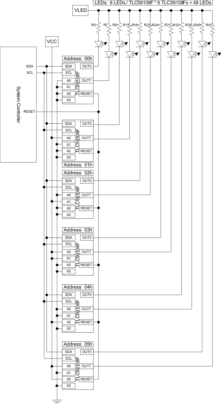 Figure 22. Six Drivers
9.2 Typical Application
This application example provides guidance on how to set the LED current using the TLC59108F.
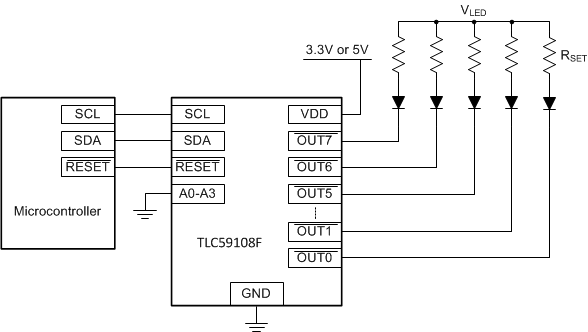 Figure 23. Typical Application
9.2.1 Design Requirements
For this design example, use the following as the input parameters listed in Table 11.
Table 11. Design Parameters
| DESIGN PARAMETERS | EXAMPLE VALUE | |||
|---|---|---|---|---|
| VLED | Supply voltage that powers LED | 5 V | ||
| VF | Forward voltage across the LED | 3 V | ||
| ILED | Current flowing through the LED | 6 mA | ||
| RON | Resistance across open-drain output | 1.5 Ω | ||
9.2.2 Detailed Design Procedure
In the LED current path, there are three voltage drops that must be considered:
- Drop across the series resistor (VRSET)
- Drop across the LED (VF)
- Drop across the open-drain output channel (VO)
The drop across the LED is defined above as VF = 3 V. The drop across the open-drain output is calculated as RON × ILED (1.5 × 0.006 = 0.009 V). The remaining voltage must be across the series resistor:
After calculating VRSET, we can calculate RSET using Equation 5, Equation 6, and Equation 7 :
9.2.3 Application Curve
The following graph shows the typical LED Current as a function of RSET and VF. The graph assumes that VLED = 5 V.
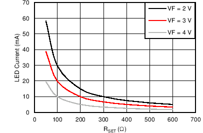 Figure 24. LED Current vs RSET