SCLS715A March   2009  – November 2015 TLC59208F

PRODUCTION DATA.  

  1. Features
  2. Applications
  3. Description
  4. Revision History
  5. Description (continued)
  6. Pin Configuration and Functions
  7. Specifications
    1. 7.1 Absolute Maximum Ratings
    2. 7.2 ESD Ratings
    3. 7.3 Recommended Operating Conditions
    4. 7.4 Thermal Information
    5. 7.5 Electrical Characteristics
    6. 7.6 I2C Interface Timing Requirements
    7. 7.7 Typical Characteristics
  8. Parameter Measurement Information
  9. Detailed Description
    1. 9.1 Overview
    2. 9.2 Functional Block Diagram
    3. 9.3 Feature Description
      1. 9.3.1 Power-On Reset
      2. 9.3.2 External Reset
      3. 9.3.3 Software Reset
      4. 9.3.4 Individual Brightness Control With Group Dimming/Blinking
    4. 9.4 Device Functional Modes
    5. 9.5 Programming
      1. 9.5.1 Characteristics of the I2C Bus
        1. 9.5.1.1 Bit Transfer
        2. 9.5.1.2 Start and Stop Conditions
      2. 9.5.2 System Configuration
      3. 9.5.3 Acknowledge
      4. 9.5.4 Device Address
      5. 9.5.5 Regular I2C Bus Slave Address
        1. 9.5.5.1 Regular I2C Bus Slave Address
      6. 9.5.6 LED All Call I2C Bus Address
      7. 9.5.7 LED Sub Call I2C Bus Address
      8. 9.5.8 Software Reset I2C Bus Address
      9. 9.5.9 Control Register
    6. 9.6 Register Maps
      1. 9.6.1 Register Descriptions
        1. 9.6.1.1 Mode Register 1 (MODE1)
        2. 9.6.1.2 Mode Register 2 (MODE2)
        3. 9.6.1.3 Individual Brightness Control Registers (PWM0-PWM7)
        4. 9.6.1.4 Group Duty Cycle Control Register (GRPPWM)
        5. 9.6.1.5 Group Frequency Register (GRPFREQ)
        6. 9.6.1.6 LED Driver Output State Registers (LEDOUT0, LEDOUT1)
        7. 9.6.1.7 I2C Bus Sub-Address Registers 1 to 3 (SUBADR1-SUBADR3)
        8. 9.6.1.8 LED All Call I2C Bus Address Register (ALLCALLADR)
  10. 10Application and Implementation
    1. 10.1 Application Information
      1. 10.1.1 Setting LED Current
      2. 10.1.2 PWM Brightness Dimming
    2. 10.2 Typical Application
      1. 10.2.1 Design Requirements
      2. 10.2.2 Detailed Design Procedure
      3. 10.2.3 Application Curve
  11. 11Power Supply Recommendations
  12. 12Layout
    1. 12.1 Layout Guidelines
    2. 12.2 Layout Example
  13. 13Device and Documentation Support
    1. 13.1 Trademarks
    2. 13.2 Community Resources
    3. 13.3 Electrostatic Discharge Caution
    4. 13.4 Glossary
  14. 14Mechanical, Packaging, and Orderable Information

Package Options

Mechanical Data (Package|Pins)
Thermal pad, mechanical data (Package|Pins)
Orderable Information

8 Parameter Measurement Information
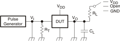
TLC59208F pmi_test_cx_cls715.gif

NOTE:

RL = Load resistance for SDA and SCL; should be >1 kΩ at 3-mA or lower current.
CL = Load capacitance; includes jig and probe capacitance.
RT = Termination resistance; should be equal to the output impedance (ZO) of the pulse generator.
Figure 6. Test Circuit for Switching Characteristics