SCLS711A March 2009 – November 2015 TLC59210
PRODUCTION DATA.
- 1 Features
- 2 Applications
- 3 Description
- 4 Revision History
- 5 Pin Configuration and Functions
-
6 Specifications
- 6.1 Absolute Maximum Ratings
- 6.2 ESD Ratings
- 6.3 Recommended Operating Conditions
- 6.4 Thermal Information
- 6.5 Electrical Characteristics: VCC = 4.5 V to 5.5 V
- 6.6 Electrical Characteristics: VCC = 3 V to 3.6 V
- 6.7 Timing Requirements: VCC = 4.5 V to 5.5 V
- 6.8 Timing Requirements: VCC = 3 V to 3.6 V
- 6.9 Switching Characteristics: VCC = 4.5 V to 5.5 V
- 6.10 Switching Characteristics: VCC = 3 V to 3.6 V
- 6.11 Typical Characteristics
- 7 Parameter Measurement Information
- 8 Detailed Description
- 9 Application and Implementation
- 10Power Supply Recommendations
- 11Layout
- 12Device and Documentation Support
- 13Mechanical, Packaging, and Orderable Information
Package Options
Mechanical Data (Package|Pins)
Thermal pad, mechanical data (Package|Pins)
Orderable Information
9 Application and Implementation
NOTE
Information in the following applications sections is not part of the TI component specification, and TI does not warrant its accuracy or completeness. TI’s customers are responsible for determining suitability of components for their purposes. Customers should validate and test their design implementation to confirm system functionality.
9.1 Application Information
In an LED display application, TLC59210 is used to drive the current sink for 8 LEDs in parallel. LED display patterns can be created by providing different bit patterns. Each LED can be duty cycled by either duty cycling the LED supply or the control bit.
9.1.1 Setting LED Current
The LED current is primarily dependent on the supply voltage, the forward voltage of the LED, and the series resistor (RSET). In many applications the supply voltage and LED forward voltage cannot be adjusted. Hence, RSET is utilized to adjust the LED current.
9.1.2 PWM Brightness Dimming
The perceived brightness of the LEDs can be adjusted by use of PWM dimming. For example, an LED driven at 50% duty cycle will appear less bright than it would at 100% duty cycle.
9.2 Typical Application
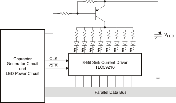
 Figure 8. Typical Application Schematic
9.2.1 Design Requirements
For an LED display application, a parallel data bus used to provide the input control for TLS59210. A character generator circuit and LED power circuit are used to generate the bit pattern written into the TLC59210 to provide the power control for the entire LED array. The LED power circuit controls the total current into the array and can also power cycle the LED array. For simple implementation, LED power circuit could be eliminated. The VLEDcan be connected directly to the resistor and LED string.
9.2.2 Detailed Design Procedure
The combination of LED Supply voltage (VLED), the LED forward voltage (VF), and external resistor sets the maximum LED current (IDS) that would appear with a 100% duty cycle.
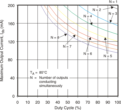
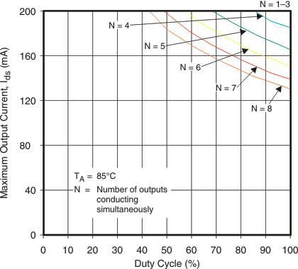
The maximum total power dissipation and maximum current through each channel of TLC59210 is determined by the number of the LEDs that are on at one time, the LED duty cycle, and the ambient temperature. The following graphs show how the maximum channel current may be limited by the total power dissipation.
9.2.3 Application Curves
 Maximum Output Current vs Duty Cycle
(TSSOP (PW) Package)
 Maximum Output Current vs Duty Cycle
 (DIP (N) Package)