SCLS711A March 2009 – November 2015 TLC59210
PRODUCTION DATA.
- 1 Features
- 2 Applications
- 3 Description
- 4 Revision History
- 5 Pin Configuration and Functions
-
6 Specifications
- 6.1 Absolute Maximum Ratings
- 6.2 ESD Ratings
- 6.3 Recommended Operating Conditions
- 6.4 Thermal Information
- 6.5 Electrical Characteristics: VCC = 4.5 V to 5.5 V
- 6.6 Electrical Characteristics: VCC = 3 V to 3.6 V
- 6.7 Timing Requirements: VCC = 4.5 V to 5.5 V
- 6.8 Timing Requirements: VCC = 3 V to 3.6 V
- 6.9 Switching Characteristics: VCC = 4.5 V to 5.5 V
- 6.10 Switching Characteristics: VCC = 3 V to 3.6 V
- 6.11 Typical Characteristics
- 7 Parameter Measurement Information
- 8 Detailed Description
- 9 Application and Implementation
- 10Power Supply Recommendations
- 11Layout
- 12Device and Documentation Support
- 13Mechanical, Packaging, and Orderable Information
Package Options
Mechanical Data (Package|Pins)
Thermal pad, mechanical data (Package|Pins)
Orderable Information
8 Detailed Description
8.1 Overview
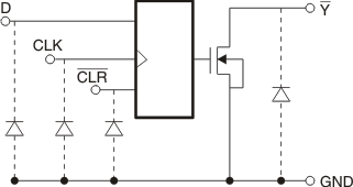
The TLC59210 is an 8-bit flip-flop driver for LED and solenoid with Schmitt-trigger buffers. Each output channel is controlled by a positive-edge-triggered D-type flip-flops with a direct clear (CLR) input. Information at the data (D) input meeting the setup time requirements is transferred to the Y output on the positive-going edge of the clock (CLK) pulse. Clock triggering occurs at a particular voltage level and is not directly related to the transition time of the positive-going pulse. When CLK is at either the high or low level, the D input has no effect at the output.
8.2 Functional Block Diagram
 Figure 6. Output Schematic

8.3 Feature Description
The TLC59210 features the ability to independently control 8 Sinking Outputs (Y). At each CLK pulse the output can be latched high or low depending on the input state (D). The CLR function allows for all outputs to be set high.
8.4 Device Functional Modes
Table 1. Function Table
(Each Latch)(1)
| INPUTS | OUTPUT Y |
||
|---|---|---|---|
| CLR | CLK | D | |
| L | X | X | H* |
| H | ↑ | L | H* |
| H | ↑ | H | L |
| H | L | X | Y0 |
| H | ↓ | X | Y0 |