SLVS867B May 2009 – August 2015 TLC59213 , TLC59213A
PRODUCTION DATA.
- 1 Features
- 2 Applications
- 3 Description
- 4 Revision History
- 5 Pin Configuration and Functions
- 6 Specifications
- 7 Parameter Measurement Information
- 8 Detailed Description
- 9 Application and Implementation
- 10Power Supply Recommendations
- 11Layout
- 12Device and Documentation Support
- 13Mechanical, Packaging, and Orderable Information
Package Options
Mechanical Data (Package|Pins)
Thermal pad, mechanical data (Package|Pins)
Orderable Information
9 Application and Implementation
NOTE
Information in the following applications sections is not part of the TI component specification, and TI does not warrant its accuracy or completeness. TI’s customers are responsible for determining suitability of components for their purposes. Customers should validate and test their design implementation to confirm system functionality.
9.1 Application Information
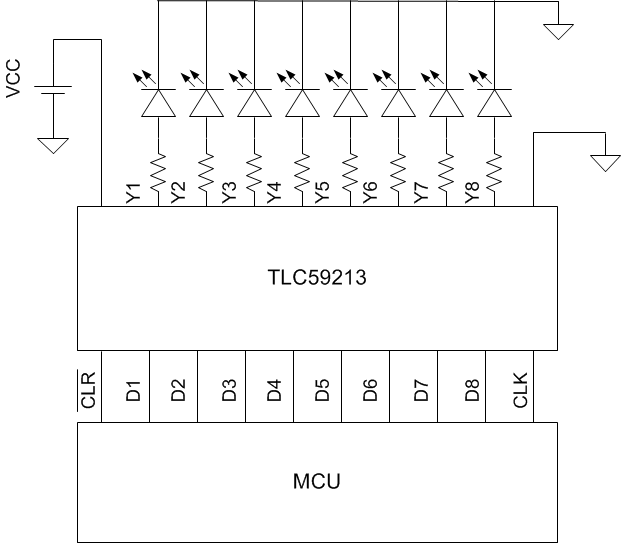
In LED display application, TLC59213 is used to drive the current source for 8 LEDs in parallel. LED display pattern can be created by providing different bit pattern. At every positive clock edge, new bit pattern will be transferred to LED display.
9.2 Typical Application
 Figure 4. Typical Application Diagram
9.2.1 Design Requirements
For LED display application, LED is selected based on the application. The current level is determined by the required brightness. Given the available supply, the resistor value could be determined. The maximum output current is constrained by the duty cycle. See Figure 1 and Figure 2.
9.2.2 Detailed Design Procedure
The selection of supply voltage (VCC), LED, and resistor sets the current of the LED.
VR is the voltage drop across the resistor, VL is the voltage drop across the LED when LED is on, VCE is the collector-to-emitter voltage of the Darlington current source driver, when the driver is enabled. For example, when VCC = 12 V, VL = 2.9 V, and VCE = 1.6 V, a 75-Ω resistor is used to obtain output current 100 mA.
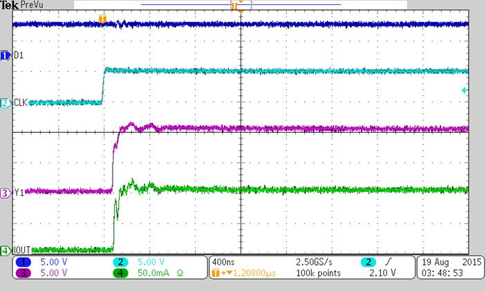
9.2.3 Application Curve
