SBVS199C June 2012 – January 2024 TLC59283
PRODUCTION DATA
- 1
- 1 Features
- 2 Applications
- 3 Description
- 4 Pin Configurations
- 5 Specifications
- 6 Parameter Measurement Information
- 7 Detailed Description
- 8 Register Configuration
- 9 Application and Implementation
- 10Device and Documentation Support
- 11Revision History
- 12Mechanical, Packaging, and Orderable Information
Package Options
Mechanical Data (Package|Pins)
Thermal pad, mechanical data (Package|Pins)
Orderable Information
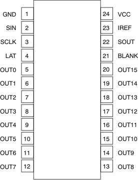
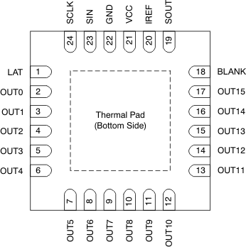
4 Pin Configurations
 Figure 4-1 DBQ PackageSSOP-24 and
QSOP-24(top
view)
 Figure 4-2 RGE PackageQFN-24(top view)
NOTE: Thermal pad is not connected to GND
internally. The thermal pad must be connected to
GND with the printed circuit board (PCB)
pattern.
Table 4-1 Pin
Functions
| PIN | I/O | DESCRIPTION | ||
|---|---|---|---|---|
| NAME | NUMBER | |||
| DBQ | RGE | |||
| BLANK | 21 | 18 | I | All outputs empty (blank); Schmitt buffer input. When BLANK is high, all constant-current outputs (OUT0 to OUT15) are forced off and all pre-charge FETs are turned on. When BLANK is low, all constant-current outputs are controlled by the data in the output on or off data latch and all pre-charge FETs are turned off. This pin is internally pulled up to VCC with a 500kΩ (typ) resistor. |
| GND | 1 | 22 | — | Power ground |
| IREF | 23 | 20 | I/O | Constant-current value setting, the OUT0 to OUT15 sink constant-current outputs are set to the desired values by connecting an external resistor between IREF and GND. |
| LAT | 4 | 1 | I | Level-triggered latch; Schmitt buffer input. The data in the 16-bit shift register continue to transfer to the output on or off data latch while LAT is high. Therefore, if the data in the 16-bit shift register are changed when LAT is high, the data in the data latch are also changed. The data in the data latch are held when LAT is low. This pin is internally pulled down to GND with a 500kΩ (typ) resistor. |
| OUT0 | 5 | 2 | O | Constant-current output. Each output can be tied together with others to increase the constant-current. Different voltages can be applied to each output. |
| OUT1 | 6 | 3 | O | Constant-current output |
| OUT2 | 7 | 4 | O | Constant-current output |
| OUT3 | 8 | 5 | O | Constant-current output |
| OUT4 | 9 | 6 | O | Constant-current output |
| OUT5 | 10 | 7 | O | Constant-current output |
| OUT6 | 11 | 8 | O | Constant-current output |
| OUT7 | 12 | 9 | O | Constant-current output |
| OUT8 | 13 | 10 | O | Constant-current output |
| OUT9 | 14 | 11 | O | Constant-current output |
| OUT10 | 15 | 12 | O | Constant-current output |
| OUT11 | 16 | 13 | O | Constant-current output |
| OUT12 | 17 | 14 | O | Constant-current output |
| OUT13 | 18 | 15 | O | Constant-current output |
| OUT14 | 19 | 16 | O | Constant-current output |
| OUT15 | 20 | 17 | O | Constant-current output |
| SCLK | 3 | 24 | I | Serial data shift
clock; Schmitt buffer input. All data in the 16-bit shift register are shifted toward the MSB by a 1-bit SCLK synchronization. |
| SIN | 2 | 23 | I | Serial data input for
driver on or off control; Schmitt buffer input.
When SIN is high, the LSB is set to '1' for only one SCLK input rising edge. If two SCLK rising edges are input while SIN is high, then the 16-bit shift register LSB and LSB+1 are set to '1'. When SIN is low, the LSB is set to '0' at the SCLK input rising edge. |
| SOUT | 22 | 19 | O | Serial data output. This output is connected to the 16-bit shift register MSB. SOUT data changes at the SCLK rising edge. |
| VCC | 24 | 21 | — | Power-supply voltage |