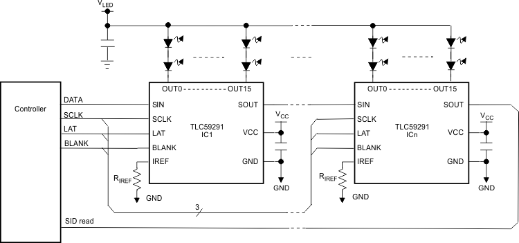
The TLC59291 is a 8/16-channel constant current sink LED driver. Each channel can be turned on-off by writing data to an internal register. The constant current value of all 16 channels is set by a single external resistor and 128 steps for the global brightness control (BC).
The TLC59291 has six type error flags: LED open detection (LOD), LED short detection (LSD), output leak detection (OLD), reference terminal short detection (ISF), Pre thermal warning (PTW) and thermal error flag (TEF). In addition, the LOD and LSD functions have invisible detection mode (IDM) that can detect those errors even when the output is off. The error detection results can be read via a serial interface port.
The TLC59291 has low quiescent current in normal mode, it also has a power-save mode that sets the total current consumption to 10 uA (typical) when all outputs are off.
PART NUMBER | PACKAGE | BODY SIZE (NOM) |
---|---|---|
TLC59291 | VQFN (24) | 4.00mm x 4.00mm |
Changes from * Revision (September 2015) to A Revision
PIN | I/O | DESCRIPTION | |
---|---|---|---|
NAME | NO. | ||
BLANK | 18 | I | BLANK PIN, has two configures: When FC9(BLANK Mode) = 0, Blank pin worked as SOUT select pin:
When FC9(BLANK Mode) = 1, Blank pin worked as OUTPUT enable pin;
|
GND | 22 | — | Ground |
IREF | 20 | I/O | Maximum current programming terminal. A resistor connected between IREF and GND sets the maximum current for every constant-current output. When this terminal is directly connected to GND, all outputs are forced off. The external resistor should be placed close to the device and must be in the range of 1.32 kΩ to 66 kΩ. |
LAT | 1 | I | Data latch. The rising edge of LAT latches the data from the common shift register into the output on/off data latch. At the same time, the data in the common shift register are replaced with SID, which is selected by SIDLD. See the Output On/Off Data Latch section and Status Information Data (SID) section for more details. |
OUT0 | 2 | O | Constant-current sink outputs. Multiple outputs can be configured in parallel to increase the constant-current capability. Different voltages can be applied to each output. |
OUT1 | 3 | O | |
OUT2 | 4 | O | |
OUT3 | 5 | O | |
OUT4 | 6 | O | |
OUT5 | 7 | O | |
OUT6 | 8 | O | |
OUT7 | 9 | O | |
OUT8 | 10 | O | |
OUT9 | 11 | O | |
OUT10 | 12 | O | |
OUT11 | 13 | O | |
OUT12 | 14 | O | |
OUT13 | 15 | O | |
OUT14 | 16 | O | |
OUT15 | 17 | O | |
SCLK | 24 | I | Serial data shift clock. Data present on SIN are shifted to the LSB of the 16-bit shift register with the SCKI rising edge. Data in the shift register are shifted toward the MSB at each SCLK rising edge. The MSB data of the common shift register appear on SOUT. |
SIN | 23 | I | Serial data input for the 16-bit common shift register. When SIN is high, a '1' is written to the LSB of the common shift register at the rising edge of SCLK. |
SOUT | 19 | O | Serial data output of the 16-bit common shift register. When FC9(BLANK Mode) = 0 and BLANK = LOW; SOUT is connected to the bit 7 of the 16-bit shift register. Data are clocked out at the SCLK rising edge. In other case: SOUT is connected to the bit 15 of the 16-bit shift register. Data are clocked out at the SCLK rising edge. |
VCC | 21 | — | Power-supply voltage |
VALUE | UNIT | |||
---|---|---|---|---|
MIN | MAX | |||
Supply voltage, VCC(2) | –0.3 | 6 | V | |
Input voltage | SIN, SCLK, LAT, BLANK, IREF | –0.3 | VCC + 0.3 | V |
Output voltage | SOUT | –0.3 | VCC + 0.3 | V |
OUT0 to OUT15 | –0.3 | 11 | V | |
Output current (DC) | OUT0 to OUT15 | 65 | mA | |
Operating junction temperature, TJ (max) | 150 | °C | ||
Storage temperature, TSTG | –55 | 150 | °C |
VALUE | UNIT | |||
---|---|---|---|---|
V(ESD) | Electrostatic discharge | Human-body model (HBM), per ANSI/ESDA/JEDEC JS-001(1) | ±4000 | V |
Charged-device model (CDM), per JEDEC specification JESD22-C101(2) | ±2000 |
PARAMETER | TEST CONDITIONS | MIN | NOM | MAX | UNIT | ||
---|---|---|---|---|---|---|---|
DC Characteristics: VCC = 3 V to 5.5 V | |||||||
VCC | Supply voltage | 3 | 3.3 | 5.5 | V | ||
VO | Voltage applied to output | OUT0 to OUT15 | 10 | V | |||
VIH | High-level input voltage | SIN, SCLK, LAT, BLANK | 0.7 × VCC | VCC | V | ||
VIL | Low-level input voltage | SIN, SCLK, LAT, BLANK | GND | 0.3 × VCC | V | ||
IOH | High-level output current | SOUT | –2 | mA | |||
IOL | Low-level output current | SOUT | 2 | mA | |||
IOLC | Constant output sink current | OUT0 to OUT15 | 3 V ≤ VCC ≤ 3.6 V | 40 | mA | ||
OUT0 to OUT15 | 3.6 V < VCC ≤ 5.5 V | 50 | mA | ||||
TA | Operating free-air temperature range | –40 | 85 | °C | |||
TJ | Operating junction temperature range | –40 | 125 | °C | |||
AC Characteristics: VCC = 3 V to 5.5 V | |||||||
fCLK (SCLK) | Data shift clock frequency | SCLK | 33 | MHz | |||
tWH0 | Pulse duration (see Figure 1 and Figure 3) |
SCLK | 10 | ns | |||
tWL0 | SCLK | 10 | ns | ||||
tWH1 | LAT | 20 | ns | ||||
tWH2 | BLANK | 40 | ns | ||||
tWL2 | BLANK | 40 | ns | ||||
tSU0 | Setup time (see Figure 1, Figure 3 and Figure 4) |
SIN to SCLK↑ | 5 | ns | |||
tSU1 | LAT↑ to SCLK↑ | 200 | ns | ||||
tSU2 | SCLK ↓to LAT↑ | 10 | ns | ||||
tH0 | Hold time (see Figure 1, Figure 3, and Figure 13) |
SIN to SCLK↑ | 3 | ns | |||
tH1 | LAT↑ to SCLK↑ | 10 | ns | ||||
tH2 | LAT↑ to SCLK ↓ | 40 | ns |
THERMAL METRIC(1) | TLC59291 | UNIT | |
---|---|---|---|
RGE (VQFN) | |||
24 PINS | |||
RθJA | Junction-to-ambient thermal resistance | 38.1 | °C/W |
RθJC(top) | Junction-to-case (top) thermal resistance | 45.3 | |
RθJB | Junction-to-board thermal resistance | 16.9 | |
ψJT | Junction-to-top characterization parameter | 0.9 | |
ψJB | Junction-to-board characterization parameter | 16.9 | |
RθJC(bot) | Junction-to-case (bottom) thermal resistance | 6.2 |
PARAMETER | TEST CONDITIONS | MIN | TYP | MAX | UNIT | ||
---|---|---|---|---|---|---|---|
VOH | High-level output voltage | IOH = –2 mA at SOUT | VCC – 0.4 | VCC | V | ||
VOL | Low-level output voltage | IOL = 2 mA at SOUT | 0.4 | V | |||
VLOD | LED open detection threshold | All OUTn = on | 0.25 | 0.30 | 0.35 | V | |
VLSD0 | LED short detection threshold | All OUTn = on, detection voltage code = 0h | 0.32 × VCC | 0.35 × VCC | 0.38 × VCC | V | |
VLSD1 | All OUTn = on, detection voltage code = 1h | 0.42 × VCC | 0.45 × VCC | 0.48 × VCC | V | ||
VLSD2 | All OUTn = on, detection voltage code = 2h | 0.52 × VCC | 0.55 × VCC | 0.58 × VCC | V | ||
VLSD3 | All OUTn = on, detection voltage code = 3h | 0.62 × VCC | 0.65 × VCC | 0.68 × VCC | V | ||
VIREF | Reference voltage output | RIREF = 1.3 kΩ | 1.175 | 1.205 | 1.235 | V | |
IIN | Input current | VIN = VCC or GND at SIN, SCLK, LAT, and BLANK | –1 | 1 | μA | ||
ICC0 | Supply current (VCC) | SIN/SCLK/LAT = Low, BLANK = High, all OUTn = off, VOUTn = 0.8 V, BC = 7Fh, RIREF = open |
2 | 3 | mA | ||
ICC1 | SIN/SCLK/LAT = Low, BLANK = High, all OUTn = off, VOUTn = 0.8 V, BC = 7Fh, RIREF = 3.6 kΩ (IOUT = 18.3 mA target) |
5 | 7 | mA | |||
ICC2 | SIN/SCLK/LAT/BLANK =Low, All OUTn = on, VOUTn = 0.8 V, BC = 7Fh, RIREF = 3.6 kΩ (IOUT = 18.3 mA target) |
5 | 7 | mA | |||
ICC3 | SIN/SCLK/LAT/BLANK =Low, All OUTn = on, VOUTn = 0.8 V, BC = 0Eh, RIREF = 1.6 kΩ (IOUT = 2 mA target) |
3 | 4 | mA | |||
ICC4 | SIN/SCLK/LAT/BLANK = Low, All OUTn = on, VOUTn = 0.8 V, BC = 7Fh, RIREF = 1.6 kΩ (IOUT = 41.3 mA target) |
9 | 11 | mA | |||
ICC5 | VCC = 5 V, SIN/SCLK/LAT/BLANK = Low, All OUTn = on, VOUTn = 0.8 V, BC = 7Fh, RIREF = 1.3 kΩ (IOUT = 50.8 mA target) |
11 | 14 | mA | |||
ICC6 | VCC = 5 V, SIN/SCLK/LAT/BLANK = Low, VOUTn = 0.8 V, BC = 7Fh, RIREF = 1.3 kΩ (IOUT = 50.8 mA target), all output data off with power-save mode enabled |
10 | 40 | µA | |||
IOL(C0) | Constant output sink current (OUT0 to OUT15, see Figure 28) |
All OUTn = on, VOUTn = VOUTfix = 0.8 V, BC = 7Fh, RIREF = 1.6 kΩ |
38.5 | 41.3 | 44.1 | mA | |
IOL(C1) | VCC = 5 V, All OUTn = on, VOUTn = VOUTfix = 1 V, BC = 7Fh, RIREF = 1.3 kΩ |
47.3 | 50.8 | 54.3 | mA | ||
IOL(KG0) | Output leakage current (OUT0 to OUT15, see Figure 28) |
BLANK = high, VOUTn = VOUTfix = 10 V, RIREF = 1.6 kΩ | TJ = 25°C | 0.1 | μA | ||
IOL(KG1) | TJ = 85°C(1) | 0.2 | μA | ||||
IOL(KG2) | TJ = 125°C(1) | 0.3 | 0.8 | μA | |||
ΔIO(LC0) | Constant-current error (channel-to-channel, OUT0 to OUT15)(2) |
All OUTn = on, VOUTn = VOUTfix = 0.8 V, BC = 0Eh, RIREF = 3.6 kΩ, TA = 25°C |
±3% | ±6% | |||
ΔIOL(C1) | Constant-current error (device-to-device, OUT0 to OUT15)(3) |
All OUTn = on, VOUTn = VOUTfix = 0.8 V, BC = 7Fh, RIREF = 1.6 kΩ, TA = 25°C |
±1% | ±3% | |||
ΔIOL(C2) | Line regulation(4) | All OUTn = on, VOUTn = VOUTfix = 0.8 V, BC = 7Fh, RIREF = 1.6 kΩ |
±0.1 | ±1 | %/V | ||
ΔIOL(C3) | Load regulation(5) | All OUTn = on, VOUTn = 0.8 V to 3 V, VOUTfix = 0.8 V, BC = 7Fh, RIREF = 1.6 kΩ |
±0.5 | ±3 | %/V | ||
TTEF | Thermal error flag threshold | Junction temperature(1) | 150 | 165 | 180 | °C | |
THYS | Thermal error flag hysteresis | Junction temperature(1) | 5 | 10 | 20 | °C | |
TPTW | Pre-thermal warning threshold | Junction temperature(1) | 125 | 138 | 150 | °C |
PARAMETER | TEST CONDITIONS | MIN | TYP | MAX | UNIT | |
---|---|---|---|---|---|---|
tR0 | Rise time | At SOUT | 10 | 15 | ns | |
tR1 | At OUTn, BC = 7Fh | 40 | 60 | ns | ||
tF0 | Fall time | At SOUT | 10 | 15 | ns | |
tF1 | At OUTn, BC = 7Fh | 40 | 60 | ns | ||
tD0 | Propagation delay | SCLK↑ to SOUT↑↓ | 8 | 22 | ns | |
tD1 | LAT↑ or BLANK↑↓ to OUT0 sink current on/off, BC = 7Fh |
35 | 65 | ns | ||
tD2 | OUTn on/off to OUTn + 1 on/off, BC = 7Fh | 2 | 6 | ns | ||
tD3 | LAT↑ to power-save mode by data writing for all output off | 400 | ns | |||
tD4 | SCLK↑ to normal mode operation | 100 | µs | |||
tD5 | BLANK↑↓ to SOUT↑↓ when BLANK MODE=0 | 100 | ns | |||
tON_ERR | Output on-time error(1) | Output on/off data = all '1', BLANK low pulse = 40 ns, BC = 7Fh |
–30 | 20 | ns | |
fOSC | Internal oscillator frequency | 12 | 20 | 28 | MHz |
NOINDENT:
On/off latched data is '1'.NOINDENT:
On/off latched data change from '1' to '0' at second LAT signal.NOINDENT:
On/off latched data change from '0' to '1' at second LAT signal.NOINDENT:
On/off latched data is '0'.NOINDENT:
If the on/off latched data is changed from “0” to “1” at 1’st LAT signal, changed from “1” to “0” at second LAT signal.NOINDENT:
If the on/off latched data is changed from “0” to “1” at 1’st LAT signal, changed from “1” to “1” at second LAT signal.NOINDENT:
If the on/off latched data is changed from “1” to “0” at 1’st LAT signal, changed from “0” to “1” at second LAT signal.NOINDENT:
if the on/off latched data is “0”.NOINDENT:
On/off latch data is '1'.NOINDENT:
On/off latch data change from '1' to '0' at second LAT signal.NOINDENT:
On/off latch data is change from '0' to '1' at second LAT signal.NOINDENT:
On/off latch data is '0'.VCC = 3.3 V | BC = 7Fh | RIREF = 1.58 kΩ |
VOUTn = 0.8 V |
VCC = 5 V | BC = 7Fh | RIREF = 1.28 kΩ |
VOUTn = 1 V |
RIREF = 1.28 kΩ | VOUTn = 0.8 V |
BC = 7Fh | RIREF = 1.6 kΩ | SIN = 17.5 MHz |
SCLK = 35 MHz | All Outpts on |
BC = 7Fh | RIREF = 1.6 kΩ | SIN = SCLK = Low |
Power-Save Mode |
VCC = 3.3 V | BC = 7Fh | VOUTn = 0.8 V |
VCC = 5 V | BC = 7Fh | VOUTn = 0.8 V |
50 mA = 1 V |
BC = 7Fh | VOUTn = 0.8 V | 50 mA = 1 V |
BC = 7Fh | RIREF = 1.6 kΩ | SIN = 17.5 MHz |
SCLK = 35 MHz | All Outpts on |
VCC = 3.3 V | BC = 7Fh | RIREF = 1.6 kΩ |
VLED = 5 V | RL = 100 Ω | CL = 15 pF |
NOINDENT:
CL includes measurement probe and jig capacitance.NOINDENT:
CL includes measurement probe and jig capacitance.