SBVS127E March 2009 – July 2017 TLC5951
PRODUCTION DATA.
- 1 Features
- 2 Applications
- 3 Description
- 4 Revision History
- 5 Description (Continued)
- 6 Pin Configuration and Functions
- 7 Specifications
- 8 Parameter Measurement Information
-
9 Detailed Description
- 9.1 Overview
- 9.2 Functional Block Diagram
- 9.3 Feature Description
- 9.4
Device Functional Modes
- 9.4.1 Maximum Constant Sink-Current Value
- 9.4.2 Dot Correction (DC) Function
- 9.4.3 Global Brightness Control (BC) Function
- 9.4.4 Grayscale (GS) Function (PWM Control)
- 9.4.5 Register and Data Latch Configuration
- 9.4.6 Status Information Data (SID)
- 9.4.7 Continuous Base LOD, LSD, and TEF
- 10Device and Documentation Support
- 11Mechanical, Packaging, and Orderable Information
Package Options
Mechanical Data (Package|Pins)
Thermal pad, mechanical data (Package|Pins)
Orderable Information
8 Parameter Measurement Information
8.1 Pin Equivalent Input and Output Schematic Diagrams
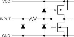 Figure 34. GSSCK, GSLAT, DCSIN, DCSCK, GSCKR, GSCKG, GSCKB
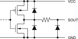 Figure 36. GSSOUT, DCSOUT
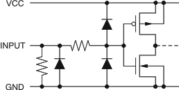 Figure 35. GSSIN, XBLNK
 Figure 37. OUTR0, -G0, -B0 Through OUTR7, -G7, -B7
8.2 Test Circuits
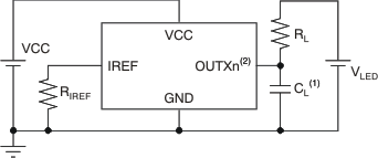
1. CL includes measurement probe and jig capacitance.
2. X = R, G, or B; n = 0–7.
Figure 38. Rise-Time and Fall-Time Test Circuit for OUTRn, -Gn, -Bn
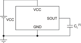
1. CL includes measurement probe and jig capacitance.
Figure 39. Rise-Time and Fall-Time Test Circuit for GSSOUT and DCSOUT
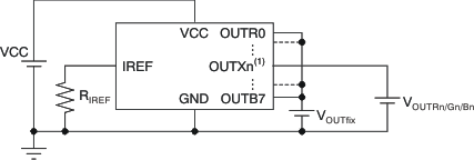
1. X = R, G, or B; n = 0–7.
Figure 40. Constant-Current Test Circuit for OUTRn, -Gn, -Bn