SLVSEJ1A February   2021  – May 2022 TLC6983

PRODUCTION DATA  

  1. Features
  2. Applications
  3. Description
  4. Revision History
  5. Description (continued)
  6. Pin Configuration and Functions
  7. Specifications
    1. 7.1 Absolute Maximum Ratings
    2. 7.2 ESD Ratings
    3. 7.3 Recommended Operating Conditions
    4. 7.4 Thermal Information
    5. 7.5 Electrical Characteristics
    6. 7.6 Timing Requirements
    7. 7.7 Switching Characteristics
    8. 7.8 Typical Characteristics
  8. Detailed Description
    1. 8.1 Overview
    2. 8.2 Functional Block Diagram
    3. 8.3 Feature Description
      1. 8.3.1 Independent and Stackable Mode
        1. 8.3.1.1 Independent Mode
        2. 8.3.1.2 Stackable Mode
      2. 8.3.2 Current Setting
        1. 8.3.2.1 Brightness Control (BC) Function
        2. 8.3.2.2 Color Brightness Control (CC) Function
        3. 8.3.2.3 Choosing BC and CC for a Different Application
      3. 8.3.3 Frequency Multiplier
      4. 8.3.4 Line Transitioning Sequence
      5. 8.3.5 Protections and Diagnostics
        1. 8.3.5.1 Thermal Shutdown Protection
        2. 8.3.5.2 IREF Resistor Short Protection
        3. 8.3.5.3 LED Open Load Detection and Removal
          1. 8.3.5.3.1 LED Open Detection
          2. 8.3.5.3.2 Read LED Open Information
          3. 8.3.5.3.3 LED Open Caterpillar Removal
        4. 8.3.5.4 LED Short/Weak Short Circuitry Detection and Removal
          1. 8.3.5.4.1 LED Short/Weak Short Detection
          2. 8.3.5.4.2 Read LED Short Information
          3. 8.3.5.4.3 LSD Caterpillar Removal
    4. 8.4 Device Functional Modes
    5. 8.5 Continuous Clock Series Interface
      1. 8.5.1 Data Validity
      2. 8.5.2 CCSI Frame Format
      3. 8.5.3 Write Command
        1. 8.5.3.1 Chip Index Write Command
        2. 8.5.3.2 VSYNC Write Command
        3. 8.5.3.3 Soft_Reset Command
        4. 8.5.3.4 Data Write Command
      4. 8.5.4 Read Command
    6. 8.6 PWM Grayscale Control
      1. 8.6.1 Grayscale Data Storage and Display
        1. 8.6.1.1 Memory Structure Overview
        2. 8.6.1.2 Details of Memory Bank
        3. 8.6.1.3 Write a Frame Data into Memory Bank
      2. 8.6.2 PWM Control for Display
    7. 8.7 Register Maps
      1. 8.7.1  FC0
      2. 8.7.2  FC1
      3. 8.7.3  FC2
      4. 8.7.4  FC3
      5. 8.7.5  FC4
      6. 8.7.6  FC10
      7. 8.7.7  FC11
      8. 8.7.8  FC12
      9. 8.7.9  FC13
      10. 8.7.10 FC14
      11. 8.7.11 FC15
  9. Application and Implementation
    1. 9.1 Application Information
    2. 9.2 Typical Application
      1. 9.2.1 Design Requirements
        1. 9.2.1.1 System Structure
        2. 9.2.1.2 SCLK Frequency
        3. 9.2.1.3 Internal GCLK Frequency
        4. 9.2.1.4 Line Switch Time
        5. 9.2.1.5 Blank Time Removal
        6. 9.2.1.6 BC and CC
      2. 9.2.2 Detailed Design Procedure
        1. 9.2.2.1 Chip Index Command
        2. 9.2.2.2 FC Registers Settings
        3. 9.2.2.3 Grayscale Data Write
        4. 9.2.2.4 VSYNC Command
        5. 9.2.2.5 LED Open and Short Read
      3. 9.2.3 Application Curves
  10. 10Power Supply Recommendations
  11. 11Layout
    1. 11.1 Layout Guidelines
    2. 11.2 Layout Example
  12. 12Device and Documentation Support
    1. 12.1 Documentation Support
      1. 12.1.1 Related Documentation
    2. 12.2 Receiving Notification of Documentation Updates
    3. 12.3 Support Resources
    4. 12.4 Trademarks
    5. 12.5 Electrostatic Discharge Caution
    6. 12.6 Glossary
  13. 13Mechanical, Packaging, and Orderable Information

Package Options

Mechanical Data (Package|Pins)
Thermal pad, mechanical data (Package|Pins)
Orderable Information

Details of Memory Bank

Each memory BANK contains the frame-image grayscale data of all the 32 lines. Each line comprises sixteen 48-bit-width memory units. Each memory unit contains the grayscale data of the corresponding R/G/B channels.

Depending on the number of scan lines set in SCAN_NUM (FC0 bit 20 to bit 16), the total number of memory units that must be written in one BANK is: 48 × the number of scan lines. For example, if the number of scan lines is set to 32, then 1536 (32 × 48 = 1536) memory units must be written during each frame period.

Figure 8-23 shows the detailed memory structure of the TLC6983 device.
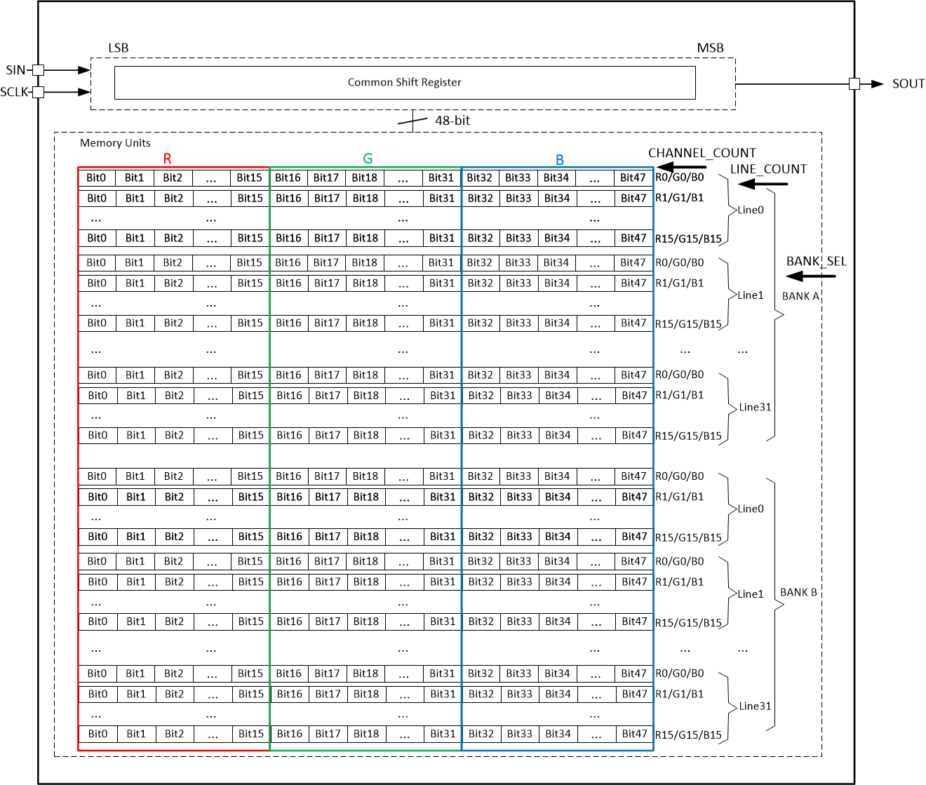
GUID-9F737A9C-CB96-4F4C-977C-8958F79A1F1F-low.gifFigure 8-23 TLC6983 Memory-unit Structure